SlideShare a Scribd company logo
1 of 180
MODULE 1
Silicon Crystal Growth
Electronic-Grade Silicon (EGS) is the raw material that is used for the preparation of single-
crystal silicon. EGS is actually a polycrystalline material of high purity. EGS has some
major impurities like boron, carbon, and residual donors. The pure EGS will have doping
elements in the parts per billion (ppb) range, and carbon less than 2 parts per million (ppm).
The step by step procedure regarding the production of EGS is shown in the block diagram
below.
Fig: Production of EGS from MGS
The process starts by the production of Metallurgical Grade Silicon (MGS) by charging it
with quartzite and carbon in an arc furnace. Quartzite is a relatively pure form of sand (SiQ2),
and carbon is obtained in the form of coal, coke, and wood chips.
The overall reaction in the furnace is given below.
SiC+Si02 = Si + SiO + CO
VLSI DESIGN
The MGS after being drawn off, has to be solidified at a purity of 98%. But this purity is not
enough for the manufacture of semiconductor devices. So, the MGS has to be pulverized
mechanically and reacted with anhydrous hydrogen chloride (HCI) to form trichlorosilane
(SiHCI3). The reaction is shown below.
Si + 3HCl = SiHCI3 + H2
With the help of a catalyst, the reaction takes place at a nominal temperature of 300°C. The
reaction creates products like silicon tetrachloride (SiCl4) and the chlorides of impurities. At
this point the purification process occurs. The purification process has to be done by
fractional distillation method as the products trichlorosilane and unwanted chlorides are
liquids at room temperature.
The purified SiHCI3 is subjected to chemical vapor deposition (CVD). The chemical
reaction is a hydrogen reduction of SiHCl3.
The chemical reaction is shown below.
2SiHCl3 + 2H2 = 2Si + 6HCl
The reaction takes place in a CVD reactor. A resistance heated Si-rod (4-mm diameter),
called a slim-rod, is used as the nucleation point for the deposition of silicon. Through the
process rods of EGC are obtained. which are up to 0.2 meters (or more) in diameter and
several meters in length. EGS can be cut from these rods as single chunks or crushed into
nuggets.
In order to achieve high overall efficiency, a feedback or recycling of reaction of by-products
is done. This is also shown in the figure above.
EGS can also be produced by pyrolysis method in which silane (SiH4) will be reacted with
heat. The reaction takes place at a high temperature of 900°C. The main advantage of using
silane instead of trichlorosilane is the lower production cost and less production of harmful
reaction by-products.
SiH4 + HEAT = Si + 2H2
In this process the CVD reactor is operated at about 900°C and supplied with silane instead
of trichlorosilane. The advantages of producing EGS from silane are lower cost and less
harmful reaction by-products.
Crystal Structure and Growing
The silicon wafermust be single crystal, but it does not represent an ideal crystal due to
following reasons:
2
VLSI DESIGN
◾The wafer has finite boundaries; thus, atoms at the surfaces are incompletely bonded as
against those in the bulk of the wafer material.
◾The atoms are displaced from their ideal locations by thermal agitation.
Czochralski Crystal Growth Process (refer written notes)
The highly refined silicon (EGS) though free from impurities, is still polycrystalline. Hence it
is to be processed to become single crystal. The Czochralski crystal growth process is often
used for producing single-crystal silicon ingots. The diagram is given below.
Since monolithic ICs are usually fabricated on a substrate which is doped with impurity, the
poly-crystalline silicon with an appropriate amount of dopant is-put into a quartz crucible,
which is then placed inside a crystal growth furnace. The material is then heated to a
temperature that is slightly in excess of the silicon melting pint of 1420 degree Celsius. A
small single-crystal rod of silicon called a seed crystal is then dipped into the silicon melt.
The conduction of heat up the seed crystal will produce a reduction in the temperature of the
melt in contact with the seed crystal to slightly below the silicon melting point. The silicon
will therefore freeze onto the end of the seed crystal, and as the seed crystal is slowly pulled
up out of the melt it will pull up with it a solidified mass of silicon that will be a
3
VLSI DESIGN
crystallographic continuation of the seed crystal. Both the seed crystal and the crucible are
rotated but in opposite directions during the crystal pulling process in order to produce
crystalline ingots of circular cross section.
The liquid solid interface remains near to the surface of the melt if the temperature and
pulling rate are correctly chosen. Even a long single crystal silicon is pulled from it. The
diameter of the ingot is controlled by the pulling rate and the melt temperature, with ingot
diameters of about 100 to 150 mm (4 to 6 inches) being the most common. The ingot length
will generally be of the order of 3 meter, and several hours are required for the “pulling” of a
complete ingot. The crystal pulling is done in an inert-gas atmosphere (usually argon or
helium), and sometimes a vacuum is used. This is done to prevent oxidation”
The pull-rate is closely related to the heat input and losses, crystal properties and dimensions.
The conditions for crystal pulling are therefore carefully controlled. For example, the melt
temperature is monitored with a thermocouple and feedback controller. Longer diameter
crystals have commercial advantages and can be grown. However, difficulties may be
encountered because of resistivity gradient across finished slices.
The crystal growth apparatus shown in the figure above consists of the following parts.
• Furnace
• Crystal pulling mechanism
• Ambient control facility
• Control system circuitry
The furnace consists of a crucible, susceptor (crucible support) and rotational mechanism,
heating element and power supply, and a chamber. As the crucible contains the melt, it is the
most important component of the growth apparatus. The crucible material should be
chemically unreactive with molten silicon. Also, the material should have high melting point,
thermal stability, and hardness. The materials for crucible, which satisfy these properties, are
silicon nitride (Si3N4) and fused silica (SiO2). The latter is in exclusive use nowadays. Fused
silica; however, reacts with silicon, releasing silicon and oxygen into the melt. In tins process
the crucible undergoes erosion. The susceptor, is used to support the silica crucible. It also
provides for better thermal conditions. Graphite is the material of choice because of its high-
temperature properties. The graphite should be pure to prevent contamination of the crystal
from impurities that would be volatilized from the graphite at the temperature involved. The
susceptor rests on a pedestal whose shaft is connected to a motor that provides rotation. The
whole assembly can usually be raised and lowered to keep the melt level equidistant from a
4
VLSI DESIGN
fixed reference point, which is needed for automatic diameter control.
The chamber housing the furnace must provide easy
access to the furnace components to facilitate maintenance and cleaning. The furnace
structure must be airtight to prevent contamination from the atmosphere, and have a specific
design that does not allow any part of the chamber to become so hot that its vapour pressure
would be a factor in contaminating the crystal. Hottest parts of the apparatus are water cooled
Insulation is usually provided between the heater and the chamber wall.
The crystal-pulling mechanism consists of seed shaft or
chain, rotation mechanism, and seed chuck. The mechanism controls two parameters of die
growth process: pull rate and crystal rotation. Also, the pulling mechanism must have
minimum vibration and great precision. The seed holder and pulling mechanism must
maintain precise orientation perpendicular to the melt surface.
From the figure shown above you can see that the crystal leaves the furnace
through a purge tube, where ambient gas, if present, is directed along the surface of the
crystal to cool it. From the purge tube, the crystal enters an upper chamber, which is usually
separated from the furnace by an isolation valve.
The ambient control for the crystal growth apparatus consists of gas source, flow
control, purge lube, and exhaust or vacuum system. The crystal growth must be conducted in
an inert gas or vacuum as staled earlier. This is necessary because
• The hot graphite parts must be protected from oxygen to prevent erosion and
• The gas around the process should not react with the molten silicon. Growth in
vacuum meets these requirements.
Growth in a gaseous atmosphere, generally used on large growers, must use an inert gas such
as helium or argon. The inert gas may be at atmospheric pressure or at reduced pressure.
The control system for crystal growing may consist of micro processing sensors, and outputs
and provides control of process parameters such as temperature, crystal diameter, pull rate
and rotation speed. The use of digital or microprocessor-based systems for control is more
common because these rely less on operator intervention and have many parts of the process
pre-programmed.
Silicon Wafer Preparation
Ingot Trimming and Slicing
As soon as the crystal ingot is obtained using the above processes, the extreme top and
bottom portions of the ingot are cut off and the ingot surface is grounded to produce a
5
VLSI DESIGN
constant and exact diameter. The normal diameter is usually 100,125, or 150 mm. A
crystallographic orientation flat is also ground along the length of the ingot. The ingot is then
sliced using a large-diameter stainless steel saw blade with industrial diamonds embedded
into the inner-diameter cutting edge. This will help in producing circular slices or wafers that
are about 600 to 1000 micro meters thick. The orientation flat serves as a useful reference
plane for various device processes.
Wafer Polishing and Cleaning
When the wafer is sliced, its surface will be heavily damaged. This can be made normal only
by polishing. The reasons for polishing are given below.
• To remove the damaged silicon from the sawn surface.
• To produce a highly planar or flat surface that will be required for the photo-
lithographic process especially when flue-line geometries are involved.
• To improve the parallel.
The sliced wafer will have saw marks and is 0.6 to 1 mm thick. This is quite rough. Hence it
has to be lapped to produce a flat surface. The wafer, before polishing, may have a surface
damage in the order of 75 micro meters. Even through lapping, only 60 micro meters can be
polished and scraped. The remaining 15 micro meters has to be removed with the help of
etching process. The chemical etch consists of an acid mixture, including nitric acid to
oxidize the surface and hydrofluoric acid to dissolve the oxide.
The wafer is then made into a mirror like finish by polishing it. This polishing is carried out
by using aluminium abrasive powders of decreasing grit size (down to a final 1 micro meters
diameter). Even after the polishing, the wafer will still have a surface damage of around 2
micro meters deep. This is removed by an additional chemical etching stage, which can
sometimes be simultaneous with the final polishing stage.
In most cases, only one side of the wafer s carefully polished to produce a mirror like image.
The other side is given a normal lapping procedure to provide a somewhat flat surface with
agreeable parallelism. After the wafer polishing operations are completed, the wafers are
thoroughly cleaned, and dried, and they are now ready to be used for the various processing
steps described in the following sections. Before discussing these steps let us discuss some
processing considerations necessary to maintain the purity and perfection of the material.
Wafer Processing Considerations
1. Chemical Cleaning
6
VLSI DESIGN
The wafers are cleaned thoroughly as soon as the polishing is completed. Originally, the
silicon wafers are cleaned so as to remove all organic films, heavy metals, and particulars:.
The commonly used cleaning agents are aqueous mixtures of NH4OH – H2O2, HCI –
H2O2,and,H2SO4-H2O2.
All of the above solutions are good enough in removing metallic impurities, but, out of the
lot, the HCI – H2O2, mixture is the best
2. Gettering Treatments
The transition group elements which act as the metallic impurities are located at the
interstitial or substitutional lattice sites and act as generation-recombination centres for the
carriers. The precipitated forms of these impurities are usually silicides. These silicides are
known to be electrically conductive . In the case of VLSI circuits, these transition group
elements decrease their performance, especially in the case of dynamic random access
memories and narrow-base bipolar transistors, as they are sensitive to conductive impurity
precipitates.
Normally, a process called gettering treatment is carried out to remove the impurities.
Gettering is a process that removes,and harms the impurities or defects them from the
regions in a wafer where devices are fabricated. Pregettering refers to a gettering treatment
provided to silicon wafers that are used for IC processing. When the wafer with sinks are
developed for device processing, the impurities are absorbed with the help of pregettering
process. The common techniques that are used for gettering treatment are given below:
• Common mechanical abrasion methods like lapping and sand blasting are carried out
to damage the back surface of the wafer.
• A focused heat beam from a Q-pulsed, Nd-YAG laser is used to damage the wafer.
Dislocations are made in the wafer by rastering the laser beam along the wafer’s back
surface. Thus they become favorable trapping sites for fast-diffusing species.
• Intrinsic gettering - As told earlier, when an impurity oxygen precipitates, defects
are generated. The defects generated by oxygen precipitation are useful as trapping
sites. As the wafer is needed for device fabrication, high temperature cycle is
employed to lower the oxygen content near the surface of the wafer. Additional
thermal cycles are added to promote the formation of oxygen precipitates and defects
in the interior of the wafer.
Diffusion of Dopant Impurities
7
VLSI DESIGN
The process of junction formation, that is transition from p to n type or vice versa, is typically
accomplished by the process of diffusing the appropriate dopant impurities in a high
temperature furnace. Impurity atoms are introduced onto the surface of a silicon wafer and
diffuse into the lattice because of their tendency to move from regions of high to low
concentration. Diffusion of impurity atoms into silicon crystal takes place only at elevated
temperature, typically 900 to 1100°C.
Although these are rather high temperatures, they are still well below the melting point of
silicon, which is at 1420°C. The rate at which the various impurities diffuse into silicon will
be of the order of 1 micro meter per hour at a temperature range stated above, and the
penetration depth that are involved in most diffusion processes will be of the order of 0.3 to
30 micro meter. At room temperature the diffusion process will be so extremely slow such
that the impurities can be considered to be essentially frozen in place.
A method of p-n junction formation which was popular in the early days is the grown
junction technique. In this method the dopant is abruptly changed in the melt during the
process of crystal growth. A convenient technique for making p-n junction is the alloying of a
metal containing doping atoms on a semiconductor with the opposite type of dopant. This is
called the alloyed junction technique. The p-n junction using epitaxial growth is widely used
in ICs. An epitaxial grown junction is a sharp junction. In terms of volume of production, the
most common technique for forming p-n junctions is the impurity diffusion process. This
produces diffused junction. Along with diffusion process the use of selective masking to
control junction geometry, makes possible the wide variety of devices available in the form
of IC’s. Selective diffusion is an important technique in its controllability, accuracy and
versatility.
Nature of Impurity Diffusion
The diffusion of impurities into a solid is basically the same type of process as occurs when
excess carriers are created non-uniformly in a semiconductor which cause carrier gradient. In
each case, the diffusion is a result of random motion, and particles diffuse in the direction of
decreasing concentration gradient The random motion of impurity atoms in a solid is, of
course, rather limited unless the temperature is high. Thus diffusion of doping impurities into
silicon is accomplished at high temperature as stated above.
There are mainly two types of physical mechanisms by which the impurities can diffuse
into the lattice. They are
1. Substitutional Diffusion
8
VLSI DESIGN
At high temperature many atoms in the semiconductor move out of their lattice site, leaving
vacancies into which impurity atoms can move. The impurities, thus, diffuse by this type of
vacancy motion and occupy lattice position in the crystal after it is cooled. Thus,
substitutional diffusion takes place by replacing the silicon atoms of parent crystal by
impurity atom. In other words, impurity atoms diffuse by moving from a lattice site to a
neighbouring one by substituting for a silicon atom which has vacated a usually occupied site
as shown in the figure below.
Substitutional diffusion mechanism is applicable to the most common diffusants, such as
boron, phosphorus, and arsenic. These dopants atoms are too big to fit into the interstices or
voids, so the only way they can enter the silicon crystal is to substitute for a Si atom.
In order for such an impurity atom to move to a neighbouring vacant site, it has to overcome
energy barrier which is due to the breaking of covalent bonds. The probability of its having
enough thermal energy to do this is proportional to an exponential function of temperature.
Also, whether it is able to move is also dependent on the availability of a vacant neighbouring
site and since an adjacent site is vacated by a Si atom due to thermal fluctuation of the lattice,
the probability of such an event is again an exponent of temperature.
The jump rate of impurity atoms at ordinary temperatures is very slow, for example about 1
jump per 1050
years at room temperature! However, the diffusion rate can be speeded up by
an increase in temperature. At a temperature of the order 1000 degree Celsius, substitutional
diffusion of impurities is practically realized in sensible time scales.
2. Interstitial Diffusion
In such, diffusion type, the impurity atom does not replace the silicon atom, but instead
moves into the interstitial voids in the lattice. The main types of impurities diffusing by such
9
VLSI DESIGN
mechanism are Gold, copper, and nickel. Gold, particularly, is introduced into silicon to
reduce carrier life time and hence useful to increase speed at digital IC’s.
Because of the large size of such metal atoms, they do not usually substitute in the silicon
lattice. To understand interstitial diffusion, let us consider a unit cell of the diamond lattice of
the silicon which has five interstitial voids. Each of the voids is big enough to contain an
impurity atom. An impurity atom located in one such void can move to a neighbouring void,
as shown in the figure below.
In doing so it again has to surmount a potential barrier due to the lattice, this time, most
neighbouring interstitial sites are vacant so the frequency of movement is reduced. Again, the
diffusion rate due to this process is very slow at room temperature but becomes practically
acceptable at normal operating temperature of around 1000 degree Celsius. It will be noticed
that the diffusion rate due to interstitial movement is much greater than for substitutional
movement. This is possible because interstitial diffusants can fit in the voids between silicon
atoms. For example, lithium acts as a donor impurity in silicon, it is not normally used
because it will still move around even at temperatures near room temperature, and thus will
not be frozen in place. This is true of most other interstitial diffusions, so long-term device
stability cannot be assured with this type of impurity.
Fick’s Laws of Diffusion
The diffusion rate of impurities into semiconductor lattice depends on the following
• Mechanism of diffusion
• Temperature
• Physical properties of impurity
• The properties of the lattice environment
10
VLSI DESIGN
• The concentration gradient of impurities
• The geometry of the parent semiconductor
The behaviour of diffusion particles is governed by Fick’s Law, which when solved for
appropriate boundary conditions, gives rise to various dopant distributions, called profiles
which are approximated during actual diffusion processes.
In 1855, Fick drew analogy between material transfer in a solution and heat transfer by
conduction. Fick assumed that in a dilute liquid or gaseous solution, in the absence of
convection, the transfer of solute atoms per unit area in a one-dimensional flow can be
described by the following equation
F = -D ∂N(x,t)/∂x = -∂F(x,t)/∂x
where F is the rate of transfer of solute atoms per unit area of the diffusion flux density
(atoms/cm2
-sec). N is the concentration of solute atoms (number of atoms per unit
volume/cm3
), and x is the direction of solute flow. (Here N is assumed to be a function of x
and t only), t is the diffusion time, and D is the diffusion constant (also referred to as
diffusion coefficient or diffusivity) and has units of cm2
/sec.
The above equation is called Fick’s First law of diffusion and states that the local rate of
transfer (local diffusion rate) of solute per unit area per unit time is proportional to the
concentration gradient of the solute, and defines the proportionality constant as the
diffusion constant of the solute. The negative sign appears due to opposite direction of
matter flow and concentration gradient. That is, the matter flows in the direction of
decreasing solute concentration.
Fick’s first law is applicable to dopant impurities used in silicon. In general the dopant
impurities are not charged, nor do they move in an electric field, so the usual drift mobility
term (as applied to electrons and holes under the influence of electric field) associated with
the above equation can be omitted. In this equation N is in general function of x, y, z and t.
The change of solute concentration with time must be the same as the local decrease of
the diffusion flux, in the absence of a source or a sink. This follows from the law of
conservation of matter. Therefore we can write down the following equation
∂N(x,t)/∂t = -∂F(x,t)/∂x
Substituting the above equation to ‘F’. We get
∂N(x,t)/∂t = ∂/∂x[D*∂N(x,t)/∂x]
When the concentration of the solute is low, the diffusion constant at a given temperature can
be considered as a constant.
Thus the equation becomes,
11
VLSI DESIGN
∂N(x,t)/∂t = D[∂2
N(x,t)/∂x2
]
This is Ficks second law of distribution.
Diffusion Profiles
Depending on boundary equations the Ficks Law has two types of solutions. These solutions
provide two types of impurity distribution namely constant source distribution following
complimentary error function (erfc) and limited source distribution following Gaussian
distribution function.
1)Constant Source (erfc) Distribution
In this impurity distribution, the impurity concentration at the semiconductor surface is
maintained at a constant level throughout the diffusion cycle. That is,
N (o,t) = NS = Constant
The solution to the diffusion equation which is applicable in this situation is most easily
obtained by first considering diffusion inside a material in which the initial concentration
changes in same plane as x=0, from NS to 0. Thus the equation can be written as
N (o,t) = NS = Constant and N(x,t) = 0
Shown below is a graph of the complementary error function for a range of values of its
argument. The change in concentration of impurities with time, as described by the equation
is also shown in the figure below. The surface concentration is always held at NS, falling to
some lower value away from the surface. If a sufficiently long time is allowed to elapse, it is
possible for the entire slice to acquire a dopant level of NS per m3
.
12
VLSI DESIGN
If the diffused impurity type is different from the resistivity type of the substrate material, a
junction is formed at the points where the diffused impurity concentration is equal to the
background concentration already present in the substrate.
In the fabrication of monolithic IC’s, constant source diffusion is commonly used for the
isolation and the emitter diffusion because it maintains a high surface concentration by a
continuous introduction of dopant.
There is an upper limit to the concentration of any impurity that can be accommodated at the
semiconductor wafer at some temperature. This maximum concentration which determines
the surface concentration in constant source diffusion is called the solid solubility of the
impurity.
2)Limited Source Diffusion or Gaussian Diffusion
Here a predetermined amount of impurity is introduced into the crystal unlike constant source
diffusion. The diffusion takes place in two steps.
1. Predeposition Step – In this step a fixed number of impurity atoms are deposited on the
silicon wafer during s short time.
2. Drive-in step – Here the impurity source is turned off and the amounts of impurities
already deposited during the first step are allowed to diffuse into silicon water.
The essential difference between the two types of diffusion techniques is that the surface
concentration is held constant for error function diffusion. It decays with time for the
Gaussian type owing to a fixed available doping concentration Q. For the case of modelling
the depletion layer of a p-n junction, the erfc is modelled as a step junction and the Gaussian
13
VLSI DESIGN
as a linear graded junction. In the case of the erfc, the surface concentration is constant,
typically the maximum solute concentration at that temperature or solid solubility limit.
Parameters which affect diffusion profile
• Solid Solubility – In deciding which of the availability impurities can be used, it is
essential to know if the number of atoms per unit volume required by the specific
profile is less than the diffusant solid solubility.
• Diffusion temperature – Higher temperatures give more thermal energy and thus
higher velocities, to the diffused impurities. It is found that the diffusion coefficient
critically depends upon temperature. Therefore, the temperature profile of diffusion
furnace must have higher tolerance of temperature variation over its entire area.
• Diffusion time – Increases of diffusion time, t, or diffusion coefficient D have
similar effects on junction depth as can be seen from the equations of limited and
constant source diffusions. For Gaussian distribution, the net concentration will
decrease due to impurity compensation, and can approach zero with increasing
diffusion tunes. For constant source diffusion, the net Impurity concentration on the
diffused side of the p-n junction shows a steady increase with time.
• Surface cleanliness and defects in silicon crystal - The silicon surface must be
prevented against contaminants during diffusion which may interfere seriously with
the uniformity of the diffusion profile. The crystal defects such as dislocation or
stacking faults may produce localized impurity concentration. This results in the
degradation of junction characteristics. Hence silicon crystal must be highly perfect.
Basic Properties of the Diffusion Process
Following properties could be considered for designing and laying out ICs.
• When calculating the total effective diffusion time for given impurity profile, one
must consider the effects of subsequent diffusion cycles.
• The erfc and Gaussian functions show that the diffusion profiles are functions of (x/
√Dt). Hence, for a given surface and background concentration, the junction depth x1
and x2 associated with the two separate diffusions having different times and
temperature
• Lateral Diffusion Effects – The diffusions proceed sideways from a diffusion
window as well as downward. In both types of distribution function, the side diffusion
is about 75 to 80 per cent of the vertical diffusion.
Dopants and their Characteristics
14
VLSI DESIGN
The dopants selection affects IC characteristics. Boron and phosphorus are the basic dopants
of most ICs. Arsenic and antimony, which are highly soluble in silicon and diffuse slowly,
are used before epitaxial processing or as a second diffusion. Gold and silver diffuse rapidly.
They act as recombination centres and thus reduce carrier life time.
Boron is almost an exclusive choice as an acceptor impurity in silicon since other p-type
impurities have limitations as follows :
Gallium has relatively large diffusion coefficient in Si02, and the usual oxide window-
opening technique for locating diffusion would be inoperative, Indium is of little interest
because of its high acceptor level of 0.16 eV, compared with 0.01 eV for boron, which
indicates that not all such acceptors would be ionized at room temperature to produce a hole.
Aluminium reacts strongly with any oxygen that is present in the silicon lattice.
The choice of a particular n-type dopant is not so limited as for p-type materials. The n-type
impurities, such as phosphorus, antimony and arsenic, can be used at different stages of IC
processing. The diffusion constant of phosphorus is much greater than for Sb and As, being
comparable to that for boron, which leads to economies resulting from shorter diffusion
times.
Dopants in VLSI Technology
The common dopants in VLSI circuit fabrication are boron, phosphorus. and arsenic.
Phosphorus is useful not only as an emitter and base dopant, but also far gettering fast-
diffusing metallic contaminants, such as Cu and An, which cause junction leakage current
problems. Thus, phosphorus is indispensable in VLSI technology. However, n-p-n transistors
made with arsenic-diffused emitters have better low-current gain characteristics and better
control of narrow base widths than those made with phosphorus-diffused emitters. Therefore,
in V LSI, the use of phosphorus as an active dopant in small, shallow junctions and low-
temperature processing will be limited to its use as the base dopant of p-n-p device and as a
gettering agent. Arsenic is the most frequently used dopant for the source and drain regions in
n-channel MOSFETs.
Diffusion Systems
Impurities are diffused from their compound sources as mentioned above. The method
impurity delivery to wafer is determined by the nature of impurity source; Two-step diffusion
is widely technique. Using this technique, the impurity concentration and profiles can be
15
VLSI DESIGN
carefully controlled. The type of impurity distribution (erfc or Gaussian) is determined by the
choice of operating conditions.
The two-step diffusion consists of a deposition step and a drive-in step. In the former step a
constant source diffusion is carried out for a short time, usually at a relatively low
temperatures, say, 1000°C. In the latter step, the impurity supply is shutoff and the existing
dopant is allowed to diffuse into the body of the semiconductor, which is now held at a
different temperature, say 1200°C, in an oxidizing atmosphere. The oxide layer which forms
on tire surface of the wafer during this step prevents further impurities from entering, or those
already deposited, from diffusing out. The final impurity profile is a function of diffusion
condition, such as temperature, time, and diffusion coefficients, for each step.
• Diffusion Furnace
For the various types of diffusion (and also oxidation) processes a resistance-heated tube
furnace is usually used. A tube furnace has a long (about 2 to 3 meters) hollow opening into
which a quartz tube about 100,150 mm in diameter is placed as shown in the figure below.
Diffusion Furnace
The temperature of the furnace is kept about1000°C. The temperature within the quartz
furnace tube can be controlled very accurately such that a temperature within 1/2°C of the
set-point temperature can be maintained uniformly over a “hot zone” about 1 m in length.
This is achieved by three individually controlled adjacent resistance elements. The silicon
wafers to be processed are stacked up vertically into slots in a quartz carrier or “boat” and
inserted into the furnace lube.
Diffusion Of p-Type Impurity
Boron is an almost exclusive choice as an acceptor impurity in silicon. It has a moderate
diffusion coefficient, typically of order I0-16 m2/sec at 1150°C which is convenient for
precisely controlled diffusion. It has a solid solubility limit of around 5 x 1026 atoms/m3, so
16
VLSI DESIGN
that surface concentration can be widely varied, but most reproducible results are obtained
when the concentration is approximately 1024/m3, which is typical for transistor base
diffusions.
• Boron Diffusion using B2H6 (Diborane) Source
This is a gaseous source for boron. This can be directly introduced into the diffusion furnace.
A number of other gases are metered into the furnace. The principal gas flow in the furnace
will be nitrogen (N2) which acts as a relatively inert gas and is used as a carrier gas to be a
dilutent for the other more reactive gases. The N2, carrier gas will generally make up some 90
to 99 percent of the total gas flow. A small amount of oxygen and very small amount of a
source of boron will make up the rest of the gas flow. This is shown in the figure below. The
following reactions will be occurring simultaneously at the surface of the silicon wafers:
Si + 02 = SiO2 (silica glass)
2B2H6 + 302 = B2O3 (boron glass) + 6H2
This process is the chemical vapour deposition (CVD) of a glassy layer on (lie silicon surface
which is a mixture of silica glass (Si02) and boron glass (B203) is called borosilica glass
(BSG). The BSG glassy layer, shown in the figure below, is a viscous liquid at the diffusion
temperatures and the boron atoms can move around relatively easily.
Diffusion Of Dopants
Furthermore, the boron concentration in the BSG is such that the silicon surface will be
saturated with boron at the solid solubility limit throughout the time of the diffusion process
as long as BSG remains present. This is constant source (erfc) diffusion. It is often called
17
VLSI DESIGN
deposition diffusion. This diffusion step is referred as pre-deposition step in which the dopant
atoms deposit into the surface regions (say 0.3 micro meters depth) of the silicon wafers. The
BSG is preferable because it protects the silicon atoms from pitting or evaporating and acts as
a “getter” for undesirable impurities in the silicon. It is etched off before next diffusion as
discussed below.
The pre-deposition step, is followed by a second diffusion process in which the external
dopant source (BSG) is removed such that no additional dopants cuter the silicon. During this
diffusion process the dopants that are already in the silicon move further in and are thus
redistributed. The junction depth increases, and at the same time the surface concentration
decreases. This type of diffusion is called drive-in, or redistribution, or limited-source
(Gaussian diffusion).
• Boron Diffusion using BBr3i (Boron Tribromide) Source
This is a liquid source of boron. In this case a controlled flow of carrier gas (N2,) is bubbled
through boron tribromide, as shown in the figure below, which with oxygen again produces
boron trioxide (BSG) at the surface of the wafers as per following reaction :
4BBr3 + 302 = B203 + 2Br2
Diffusion of n-Type Impurity
For phosphorus diffusion such compounds as PH3 (phosphine) and POCl3 (phosphorus
oxychloride) can be used. In the case of a diffusion using PoCI3, the reactions occurring at
the silicon wafer surfaces will be:
Si + 02 = SiO2 (silica glass)
4POCl + 302 = 2P205 + 6Cl2
This will result in the production of a glassy layer on the silicon wafers (hat is a mixture of
phosphorus glass and silica glass called phosphorosilica glass (PSG), which is a viscous
liquid at the diffusion temperatures. The mobility of the phosphorus atoms in this glassy layer
and the phosphorus concentration is such that the phosphorus concentration at the silicon
surface will be maintained at the solid solubility limit throughout the time of the diffusion
process (similar processes occur with other dopants, such as the case of arsenic, in winch
arsenosilica glass is formed on the silicon surface.
The rest of the process for phosphorus diffusion is similar to boron diffusion, that is, after
deposition step, drive-in diffusion is carried out.
18
VLSI DESIGN
P205 is a solid source for phosphorus impurity and can be used in place of POCl3. However
POCl3 offers certain advantages overP205 such as easier source handling, simple furnace
requirements, similar glassware for low and high surface concentrations and better control of
impurity density from wafer to wafer and from run to run.
Ion Implantation
Ion Implantation is an alternative to a deposition diffusion and is used to produce a shallow
surface region of dopant atoms deposited into a silicon wafer. This technology has made
significant roads into diffusion technology in several areas. In this process a beam of impurity
ions is accelerated to kinetic energies in the range of several tens of kV and is directed to the
surface of the silicon. As the impurity atoms enter the crystal, they give up their energy to the
lattice in collisions and finally come to rest at some average penetration depth, called the
projected range expressed in micro meters. Depending on the impurity and its implantation
energy, the range in a given semiconductor may vary from a few hundred angstroms to about
1micro meter. Typical distribution of impurity along the projected range is approximately
Gaussian. By performing several implantations at different energies, it is possible to
synthesize a desired impurity distribution, for example a uniformly doped region.
Ion Implantation System
A typical ion-implantation system is shown in the figure below.
19
VLSI DESIGN
A gas containing the desired impurity is ionized within the ion source. The ions are generated
and repelled from their source in a diverging beam that is focussed before if passes through a
mass separator that directs only the ions of the desired species through a narrow aperture. A
second lens focuses this resolved beam which then passes through an accelerator that brings
the ions to their required energy before they strike the target and become implanted in the
exposed areas of the silicon wafers. The accelerating voltages may be from 20 kV to as much
as 250 kV. In some ion implanters, the mass separation occurs after the ions are accelerated
to high energy. Because the ion beam is small, means are provided for scanning it uniformly
across the wafers. For this purpose the focussed ion beam is scanned electrostatically over the
surface of the wafer in the target chamber.
Repetitive scanning in a raster pattern provides exceptionally uniform doping of the wafer
surface. The target chamber commonly includes automatic wafer handling facilities to speed
up the process of implanting many wafers per hour.
Properties of Ion Implantation
The depth of penetration of any particular type of ion will increase with increasing
accelerating voltage. The penetration depth will generally be in the range of 0.1 to 1.0 micro
meters.
Annealing after Implantation
After the ions have been implanted they are lodged principally in interstitial positions in the
silicon crystal structure, and the surface region into which the implantation has taken place
20
VLSI DESIGN
will be heavily damaged by the impact of the high-energy ions. The disarray of silicon atoms
in the surface region is often to the extent that this region is no longer crystalline in structure,
but rather amorphous. To restore this surface region back to a well-ordered crystalline
state and to allow the implanted ions to go into substitutional sites in the crystal
structure, the wafer must be subjected to an annealing process. The annealing process
usually involves the heating of the wafers to some elevated temperature often in the
range of 1000°C for a suitable length of time such as 30 minutes.
Laser beam and electron-beam annealing are also employed. In such annealing techniques
only the surface region of the wafer is heated and re-crystallized. An ion implantation process
is often followed by a conventional-type drive-in diffusion, in which case the annealing
process will occur as part of the drive-in diffusion.
Ion implantation is a substantially more expensive process than conventional deposition
diffusion, both in terms of the cost of the equipment and the throughput, it does, however,
offer following advantages.
Advantages of Ion Implantation
• Ion implantation provides much more precise control over the density of dopants
deposited into the wafer, and hence the sheet resistance. This is possible because both
the accelerating voltage and the ion beam current are electrically controlled outside of
the apparatus in which the implants occur. Also since the beam current can be
measured accurately during implantation, a precise quantity of impurity can be
introduced. Tins control over doping level, along with the uniformity of the implant
over the wafer surface, make ion implantation attractive for the IC fabrication, since
this causes significant improvement in the quality of an IC.
• Due to precise control over doping concentration, it is possible to have very low
values of dosage so that very large values of sheet resistance can be obtained. These
high sheet resistance values are useful for obtaining large-value resistors for ICs. Very
low-dosage, low-energy implantations are also used for the adjustment of the
threshold voltage of MOSFET’s and other applications.
• An obvious advantage of implantation is that it can be done at relatively low
temperatures, this means that doped layers can be implanted without disturbing
previously diffused regions. This means a lesser tendency for lateral spreading.
High-Current High-Energy Implantation Machines
21
VLSI DESIGN
The ion-implantation apparatus, discussed above, has limits to energy range. The minimum
implantation energy is usually set by the extraction voltage, that is, the voltage causing the
ions to move out of the ion source into the mass separator. This voltage (which is typically 20
KeV) cannot be reduced too far without drastically reducing beam current. The maximum
implantation energy is set by the design of the high voltage equipment. The only way to
circumvent this is to implant multiply-charged ions.
High beam currents are obtained by using multiple extraction electrodes and higher voltages.
To get a final beam of suitable energy a combination of acceleration and deceleration modes
of operation is used.
The electrostatic scanning is not suitable for high-beam currents, as it disrupts space charge
neutrality and leads to beam “blow-up”. Therefore a mechanical scanning system is usually
used. In this case, the wafer is scanned past a stationary beam. This method has the added
advantage of keeping the same beam angle across the whole wafer, whereas an electrostatic
system can vary by ±2° for 100 mm wafers. However, mechanical scanning puts new
requirements on the wafer holder.
High-energy implantation, at MeV energies, makes possible several new processing
techniques required for VLSI.
High-energy implantation machines however introduce high-voltage breakdown problem. At
about 400 KeV of energy electrical breakdown of the air around the high voltage equipment
occurs. Hence, above 400 KeV, conventional equipment is used. Also, high energy implants
frequently require water stages heated up to 600 degree Celsius, so that self annealing during
implantation minimizes damage in the surface layer. Mechanical scanning is used because of
the difficulty of electrostatically scanning a high-energy beam.
Problems in VLSI Processing
Now a day’s large diameter wafers are feasible. Large size wafers are necessary for VLSI.
This makes the task of uniformly implanting a wafer increasingly difficult. This in turn has
effect on sheet resistance. Ion implantation is basically clean process because contaminant
ions are separated from the beam before they hit the target. There are still several sources of
contamination possible near the end of the beam line, which can result in contaminant dose
up to 10 percent of the intended ion dose, for example, metal atoms knocked from chamber
walls, water holder, masking aperature and so on.
Annealing, as discussed earlier, is required to repair lattice damage and put dopant
atoms on substitutional site where they will be electrically active. The success of
22
VLSI DESIGN
annealing is often measured in terms of the fraction of the dopant that is electrically active, as
found experimentally using a Hall Effect technique. For VLSI, the challenge in annealing is
not simply to repair damage and activate dopant, but to do so while minimizing diffusion so
that shallow implants remain shallow. This has motivated much work in rapid thermal
annealing (RTA), where annealing times are on the order of seconds. RTA uses
tungsten-halogen lamps or graphite resistive strips to heat the wafer from one or both
sides as against conventional furnace annealing where times or on the order of minutes.
Modern device structures, such as the lightly-doped drains (LDD) for MOSFET, require
precise control of dopant distribution vertically and lateral on a very fine scale. For VLSI
CMOS structure, we need to form shallow n and layers with implantation energies within the
reach of standard machines. As stated earlier, the ion velocity, perpendicular to the surface,
determines the projected range of an implanted ion distribution. If the water is tilted at a large
angle to the ion beam then the effective ion energy is greatly reduced tilted ion beams, thus,
make it possible to achieve extremely shallow dopant distributions using comparatively high
implantation energies. We can circumvent the problem of implanting a shallow layer in
silicon completely if instead we implant entirely into a surface layer and then diffuse the
dopant into the substrate. This is most often done when the surface film is to be used as a
conductor making contact to the substrate. Diffusion results in steep dopant profiles without
damage to the silicon lattice. Dopant diffusion in silicides and polysilicon is generally much
faster than in single-crystal silicon, so the implanted atoms soon become uniformly
distributed in the film.
Importance of Ion Implantation for VLSI Technology
Ion implantation is a very popular process for VLSI because it provides more precise control
of dopants (as compared to diffusion). With the reduction of device sizes to the submicron
range, the electrical activation of ion-implanted species relies on a rapid thermal annealing
technique, resulting in as little movement of impurity atoms as possible. Thus, diffusion
process has become less important than methods for introducing impurity atoms into silicon
for forming very shallow junctions, an important feature of VLSI circuits. Ion, implantation
permits introduction of the dopant in silicon that is controllable, reproducible and free from
undesirable side effects. Over
23
VLSI DESIGN
Oxidation
The function of a layer of silicon dioxide (SiO2) on a chip is multipurpose. SiO2 plays an
important role in IC technology because no other semiconductor material has a native oxide
which is able to achieve all the properties of SiO2. The role of SiO2 in IC fabrication is as
below
• It acts as a diffusion mask permitting selective diffusions into silicon wafer through
the window etched into oxide.
• It is used for surface passivation which is nothing but creating protective SiO2 layer
on the wafer surface. It protects the junction from moisture and other atmospheric
contaminants.
• It serves as an insulator on the water surface. Its high relative dielectric constant,
which enables metal line to pass over the active silicon regions.
• SiO2 acts as the active gate electrode in MOS device structure.
• It is used to isolate one device from another.
• It provides electrical isolation of multilevel metallization used in VLSI.
It is fortunate that silicon has an easily formed protective oxide, for otherwise we should have
to depend upon deposited insulators for surface protection. Since SiO2 produces a stable
layer, this has held back germanium IC technology.
Growth and Properties of Oxide Layers on Silicon
Silicon dioxide (silica) layer is formed on the surface of a silicon wafer by thermal oxidation
at high temperatures in a stream of oxygen.
Si+02 = SiO2 (solid)
The oxidation furnace used for this reaction is similar to the diffusion furnace. The thickness
of the oxide layer depends on the temperature of the furnace, the length of time that the
wafers are in it, and the flow rate of oxygen. The rate of oxidation can be significantly
increased by adding water vapour to the oxygen supply to the oxidizing furnace.
Si + 2H2O = SiO2 + 2H2
The time and temperature required to produce a particular layer thickness arc obtained from
empirically determined design curves, of the type shown in the figures given below
corresponding to dry- oxygen atmosphere and also corresponding to steam atmosphere.
24
VLSI DESIGN
Growth and Properties of Oxide Layers on Silicon
In the past, steam was obtained by boiling ultra-high-purity water and passing it into the high-
temperature furnace containing the silicon wafers; however, present day technologies
generally use hydrogen and oxygen which are ignited in the furnace tube to form the ultra
high-purify water vapour.
The process of silicon oxidation takes place many times during the fabrication of an IC. Once
silicon has been oxidized the further growth of oxide is controlled by the thickness of the
initial or existing oxide layer.
Kinetics of oxidation
A well established model for thermal oxide growth has been proposed by Deal and Grove
Concept and Formulation (just for extra information-Not in syllabus)
If one assumes that the oxidation process is dominated by the inward movement of the
oxidant species, the transported species must go through the following stages:
(1) It is transported from the bulk of the oxidizing gas to the outer surface of oxide, where it
is adsorbed.
(2) It is transported across the oxide film towards silicon.
25
VLSI DESIGN
(3) It reacts at the interface with silicon and form a new layer of SiO2.
Each of these steps can be described as independent flux equation. The adsorption of oxidants
is written as
(1)
where is the gas-phase transport coefficient, is the equilibrium concentration of the
oxidants in the surrounding gas atmosphere, and Co is the concentration of oxidants at the
oxide surface at any given time.
It was found experimentally that wide changes in gas flow rates in the oxidation furnaces,
changes in the spacing between wafers on the carrier in the furnace, and a change in wafer
orientation (standing up or lying down) cause only little difference in oxidation rates. These
results imply that is very large, or that only a small difference between and Co is
required to provide the necessary oxidant flux.
is also the solubility limit in the oxide, which is assumed to be related to the partial
pressure p of the oxidant in the gas atmosphere by Henry's law
(2)
At natural ambient pressure of 1 atm and at a temperature of 1000 C, the solubility limits are
5.2 x10 cm for O2, and 3.0 x10 cm for H2O.
The flux F2 represents the diffusion of the oxidants through the oxide layer to the Si-SiO2
interface, which can be expressed as
(3)
where is the oxidant diffusivity in the oxide, Cs is the oxidant concentration at the oxide-
silicon interface, and xo represents the oxide thickness. In this expression it is assumed that
the process is in steady state (no changing rapidly with time), and that there is no loss of
oxidants when they diffuse through the oxide. Under these conditions, F2 must be constant
through the oxide and hence the derivative can be replaced simply by a constant gradient.The
third part of the oxidation process is the flux of oxidants consumed by the oxidation reaction
at the oxide-silicon interface given by
(4)
with ks as the surface rate constant. ks really represents a number of processes occurring at the
Si/SiO2 interface. These may include oxidant (O2 2O), Si-Si bond breaking, and/or Si-O
26
VLSI DESIGN
bond formation. The rate at which this reaction takes place should be proportional to the
oxidant concentration at the interface Cs.
Figure 2.16: One-dimensional model for the oxidation of silicon.
Deal and Grove assumed that in the steady state condition these three fluxes are equal, which
allows to express them as
(5)
The rate of oxide growth is proportional to the flux of oxidant molecules,
(6)
where N is the number of oxidant molecules incorporated per unit volume.
The differential equation can be simplified as
(7)
with the physically based parameters
(8)
(9)
Growth Rate of Silicon Oxide Layer
The initial growth of the oxide is limited by the rate at which the chemical reaction takes
place. After the first 100 to 300 A of oxide has been produced, the growth rate of the oxide
27
VLSI DESIGN
layer will be limited principally by the rate of diffusion of the oxidant (02 or H20) through the
oxide layer, as shown in the figures given below.
The rate of diffusion of O2 or H2O through the oxide layer will be inversely proportional to
the thickness of the layer, so that we will have that dx/dt = C/x
where x is the oxide thickness and C is a constant of proportionality. Rearranging this
equation gives xdx = Cdt
Integrating this equation both sides yields, x2
/2 = Ct
Solving for the oxide thickness x gives, x = √2Ct
We see that after an initial reaction-rate limited linear growth phase the oxide growth will
become diffusion-rate limited with the oxide thickness increasing as the square root of the
growth time. This is also shown in the figure below.
The rate of oxide growth using H2O as the oxidant will be about four times faster than the
rate obtained with O2. This is due to the fact that the H2O molecule is about one-half the size
of the O2 molecule, so that the rate of diffusion of H2O through the SiO2 layer will be much
greater than the O2 diffusion rate.
Oxide Charges
The interlace between silicon and silicon dioxide contains a transition region. Various
charges are associated with the oxidised silicon, some of which are related to the transition
region. A charge at the interface can induce a charge of the opposite polarity in the
underlying silicon, thereby affecting the ideal characteristics of the MOS device. This results
in both yield and reliability problems. The figure below shows general types of charges.
28
VLSI DESIGN
• Interface-trapped charges
These charges at Si-SiO2 are thought to result from several sources including structural
defects related to the oxidation process, metallic impurities, or bond breaking processes. The
density of these charges is usually expressed in terms of unit area and energy in the silicon
band gap.
• Fixed oxide charge
This charge (usually positive) is located in the oxide within approximately 30 A of the Si –
SiO2 interface. Fixed oxide charge cannot be charged or discharged. From a processing point
of view, fixed oxide charge is determined by both temperature and ambient conditions.
• Mobile ionic charge
This is attributed to alkali ions such as sodium, potassium, and lithium in the oxides as well
as to negative ions and heavy metals. The alkali ions are mobile even at room temperature
when electric fields are present.
• Oxide trapped charge
This charge may be positive or negative, due to holes or electrons trapped in the bulk of the
oxide. This charge, associated with defects in the Si02, may result from ionizing radiation,
avalanche injection.
Effect of Impurities on the Oxidation Rate
The following impurities affect the oxidation rate
1. Water
2. Sodium
3. Group III and V elements
4. Halogen
In addition damage to the silicon also affects oxidation rate. As wet oxidation occurs at a
substantially greater rate than dry oxygen, any unintentional moisture accelerates the dry
29
VLSI DESIGN
oxidation. High concentrations of sodium influence the oxidation rate by changing the bond
structure in the oxide, thereby enhancing the diffusion and concentration of the oxygen
molecules in the oxide.
During thermal oxidation process, an interface is formed, which separates the silicon from
silicon dioxide. As oxidation proceeds, this interface advances into the silicon. A doping
impurity, which is initially present in the silicon, will redistribute at the interface until its
chemical potential is the same on each side of the interface. This redistribution may result in
an abrupt change in impurity concentration across the interface. The ratio of the equilibrium
concentration of the impurity, that is, dopant in silicon to that in SiO2 at the interface is called
the equilibrium segregation coefficient. The redistribution of the dopants at the interface
influences the oxidation behaviour. If the dopant segregates into the oxide and remains there
(such as Boron, in an oxidizing ambient), the bond structure in the silica weakens. This
weakened structure permits an increased incorporation and diffusivity of the oxidizing
species through the oxide thus enhancing the oxidation rate. Impurities that segregate into the
oxide but then diffuse rapidly through it (such as aluminium, gallium, and indium) have no
effect on the oxidation kinetics. Phosphorus impurity shows opposite effect to that of boron,
that is, impurity segregation occurs in silicon rather than Si02. The same is true for As and Sb
dopants.
Halogen (such as chlorine) impurities are intentionally introduced into the oxidation ambient
to improve both the oxide and the underlying silicon properties. Oxide improvement occurs
because there is a reduction in sodium ion contamination, increase in oxide breakdown
strength, and a reduction in interface trap density. Traps arc energy levels in the forbidden
energy gap which are associated with defects in the silicon.
Growth and Properties of Thin Oxides
MOS VLSI technology requires silicon dioxide thickness in the 50 to 500 A range in a
repeatable manner. This section is devoted to the growth and properties of such thin oxide.
This oxide must exhibit good electrical properties and provide long-term reliability. As an
example, the dielectric material for MOS devices can be thin thermal oxide. This dielectric is
an active component of the storage capacitor in dynamic RAMs, and its thickness determines
the amount of charge that can be stored.
The growth of thin oxide must be slow enough to obtain uniformity and reproducibility.
Various growth techniques for thin oxide are dry oxidation, dry oxidation with HCl,
sequential oxidations using different temperatures and ambients, wet oxidation, reduced
pressure techniques, and high pressure/low temperature oxidation. High pressure oxidation is
30
VLSI DESIGN
discussed later. The oxidation rate will, of course, be lower at lower temperatures and at
reduced pressures. Ultra-thin oxide (<50 A) have been produced using hot nitric acid, boiling
water, and air at room temperatures. Some recent developments in thin oxide growth
technique are
(i) Rapid thermal oxidation performed in a controlled oxygen ambient with heating provided
by tungsten-halogen lamps and
(ii) Ultraviolet pulsed laser excitation in an oxygen environment.
The properties of thin oxide depend upon the growth technique employed. For example,
oxide density increases as the oxidation temperature is reduced. Additionally, HCl ambients
have typically been used to passivate ionic sodium, improve the breakdown voltage, and
getter impurities and defects in the silicon. This passivation effect begins to occur only in the
higher temperature range.
For thin oxides, there is an increase in leakage for a given voltage. In thin oxides the
dielectric breakdown may be field-dependent (breakdown in a ramping field) or time-
dependent (breakdown at a constant field). This breakdown is a failure mode for MOS ICs.
Thinner oxides are more prone to failure.
High Pressure Oxidation
There is a benefit of increase in the oxidation rate if the thermal oxidation is carried out at
pressures that are much above atmospheric pressure. The rate of diffusion of the oxidant
molecules through an oxide layer is proportional to the ambient pressure. For example, at a
pressure of 10 atm the diffusion rate will be increased by a factor of 10 and the corresponding
oxidation time can be reduced by nearly the same factor. Alternatively, the oxidation can be
done for the same length of time, but the temperature required will be substantially lower.
Thus, one principal benefit of high-pressure oxidation processing is lower-temperature
processing. The lower processing temperature reduces the formation of crystalline defects
and produces less effect on previous diffusions and other processes. The shorter oxidation
time is also advantageous in increasing the system throughput. The major limitation of this
process is the high initial cost of the system.
Applications
Oxide Masking
The oxide layer is used to mask an underlying silicon surface against a diffusion (or ion
implantation) process. The oxide layer is patterned by the photolithographic process to
produce regions where there are opening or “windows” where the oxide has been removal to
expose the underlying silicon. Then these exposed silicon regions are subjected to the
31
VLSI DESIGN
diffusion (or implantation) of dopants, whereas the unexposed silicon regions will be
protected. The pattern of dopant that will be deposited into the silicon will thus be a
replication of the pattern of opening in the oxide layer. The replication is a key factor in the
production of tiny electronic components.
The thickness of oxide needed for diffusion masking is a function of the type of diffusant and
the diffusion time and temperature conditions. In particular, an oxide thickness of some 5000
A will he vufftcieni to mask against almost all diffusions. This oxide thickness will also be
sufficient to block almost alt but the highest-energy ion implantation.
Oxide Passivation
The other function of Si02 in IC fabrication is the surface passivation. This is nothing but
creating protective Si02 layer on the wafer surface. The figure below shows a cross-sectional
view of a p-n junction produced by diffusion through an oxide window. There are lateral
diffusion effects, that is, the diffusion not only proceeds in the downward direction, but also
sideways as well, since diffusion is an isotropic process. The distance from the edge of the
oxide window to the junction in the lateral direction underneath die oxide is indicated as yj.
Lithography
Lithography is the process of transferring geometric shapes on a mask to the surface of a
silicon wafer. When a sample of crystalline silicon is covered with silicon dioxide, the oxide-
layer acts as a barrier to the diffusion of impurities, so that impurities separated from the
surface of the silicon by a layer of oxide do not diffuse into the silicon during high-
temperature processing.
The selective removal of the oxide in the desired area is performed with lithography. Thus,
the areas over which diffusions are effective are defined by the oxide layer with windows cut
32
VLSI DESIGN
in it, through which diffusion can take place. The windows are produced by the lithographic
process. This process is the means by which microscopically small electronic circuits and
devices can be produced on silicon wafers resulting in as many as 10000 transistors on a 1
cm x 1 cm chip.
In IC fabrication a number of masks are employed. Except for the first mask, every mask
must be aligned to the pattern produced by the previous mask. This is done using mask
aligner. The mask aligner may be contact type or proximity type or projection type.
Accordingly we have three types of printing. They are
◾Contact printing
◾Proximity printing
◾Projection printing
Photolithography
In this process the exposing radiation, such as ultraviolet (UV) light in case of
photolithography, is transmitted through the clear parts of the mask. The circuit pattern of
opaque chromium blocks some of die radiation. This type of chromium/glass mask is used
with UV light.
Photolithographic Process Steps
1. Photoresist Application (Spinning)
A drop of light-sensitive liquid called photoresist is applied to the centre of the oxidized
silicon wafer that is held down by a vacuum chuck. The wafer is then accelerated rapidly to a
rotational velocity in the range 3000 to 7000 RPM for some 30 to 60 seconds. This action
spreads the solution in a thin, nearly uniform coat and spins off the excess liquid. The
thickness of the coat so obtained is in the range 5000 to 10000 A, as shown in the figure
below. The thickness of the photoresist layer will be approximately inversely proportional to
the square root of the rotational velocity.
Sometimes prior to the application of the photoresist the silicon wafers are given a “bake-out”
at a temperature Of at least 100°C to drive off moisture from the wafer surfaces so as to
obtain better adhesion of the photoresist. Typical photoresist used is Kodak Thin Film Resist
(KTFR).
2. Prebake
The silicon wafers coated with photoresist are now put into an oven at about 80°C for about
30 to 60 minutes to drive off solvents in the photoresist and to harden it into a semisolid film.
3. Alignment and Exposure
33
VLSI DESIGN
The coated wafer, as above, is now placed in an apparatus called a mask aligner in very close
proximity (about 25 to 125 micro meters) to a photomask. The relative positions of the wafer
and the photomasks are adjusted such that the photomask is correctly lined up with reference
marks or a pre-existing pattern on the wafer.
The photomask is a glass plate, typically about 125 mm square and about 2 mm thick. The
photomask has a photographic emulsion or thin film metal (generally chromium) pattern on
one side. The pattern has clear and opaque areas. The alignment of the photomask to the
wafer is often required to be accurate to within less than 1 micro meter, and in some cases to
within 0.5 micro meters. After proper alignment has been achieved, the wafer is brought into
direct contact with the photomask. Photomask making will be described separately.
A highly collimated ultraviolet (UV) light is then turned on and the areas of the silicon wafer
that are not covered by the opaque areas of the photomask are exposed to ultraviolet
radiation, as shown in the figure. The exposure time is generally in the range 3 to 10 seconds
and is carefully controlled such that the total UV radiation dosage in watt-seconds or joules is
of the required amount.
4. Development
Two types of photoresist exist- negative photoresist and positive photoresist. In the present
description negative photoresist is used in which the areas of the photoresist that are exposed
the ultraviolet radiation become polymerized. The polymerization process increases the
length of the organic chain molecules that make up the photoresist. This makes the resist
tougher and makes it essentially insoluble in the developer solution. The resisting photoresist
pattern after the development process will therefore be a replication of the photomask pattern,
with the clear areas on the photomask corresponding to the areas where the photoresist
remains on the wafers, as shown in the figure below.
An opposite type of process occurs with positive photoresist. Exposure to UV radiation
results in depolymerization of the photoresist. This makes these exposed areas of the
photoresist readily soluble in the developer solution, whereas the unexposed areas are
essentially insoluble. The developer solution will thus remove the exposed or depolymerized
regions of the photoresist, whereas the unexposed areas will remain on the wafer. Thus again
there is a replication of the photomask pattern, but this time the clear areas of the photomask
produce the areas on the wafer from which the photoresist has been removed.
5. Postbake
After development and rinsing the wafers are usually given a postbake in an oven at a
temperature of about 150°C for about 30 to 60 minutes to toughen further the remaining resist
34
VLSI DESIGN
on the wafer. This is to make it adhere better to the wafer and to make it more resistant to the
hydrofluoric acid [HF] solution used for etching of the silicon dioxide.
6. Oxide Etching
The remaining resist is hardened and acts as a convenient mask through which the oxide layer
can be etched away to expose areas of semiconductor underneath. These exposed areas are
ready for impurity diffusion.
For etching of oxide, the wafers are immersed in or sprayed with a hydrofluoric [HF] acid
solution. This solution is usually a diluted solution of typically 10: 1, H2O : HF, or more often
a 10 : 1 NH4F [ammonium fluoride]: HF solution. The HF solutions will etch the SiO2 but
will not attack the underlying silicon, nor will it attack the photoresist layer to any
appreciable extent. The wafers are exposed to the etching solution ion enough to remove the
SiO2 completely in the areas of the wafer that are not covered by the photoresist as shown in
the figure.
The duration of oxide etching should be carefully controlled so that all of the oxide present
only in the photoresist window is removed. If etching time is excessively prolonged, it will
result in more undercutting underneath the photoresist and widening of the oxide opening
beyond what is desired.
The above oxide etching process is termed wet etching process since the chemical reagents
used are in liquid form. A newer process for oxide etching is a dry etching process called
plasma etching. Another dry etching process is ion milling.
7. Photoresist Stripping
Following oxide etching, the remaining resist is finally removed or stripped off with a
mixture of sulphuric acid and hydrogen peroxide and with the help of abrasion process.
Finally a step of washing and drying completes the required window in the oxide layer. The
figure below shows the silicon wafer ready for next diffusion.
35
VLSI DESIGN
Photolithographic Process Steps
Negative photoresists, as above, are more difficult to remove. Positive photoresists can
usually be easily removed in organic solvents such as acetone.
The photolithography may employ contact, proximity, or projection printing. For IC
production the line width limit of photolithography lies near 0.4 micro meters, although 0.2
micro meters features may be printed under carefully controlled conditions. At present, the
photolithography occupies the primary position among various lithographic techniques.
Photoresists
One of the major factors in providing increasingly complex devices has been improvement in
photolithographic art. A large part of this improvement has been due to high quality
photoresist, materials as improved techniques of coating, baking, exposing and developing
photoresists.
The principal constituents of a photoresist solution are a polymer, a sensitizer and a suitable
solvent system Polymers have properties of excellent film forming and coating. Polymers
generally used are polyvinyl cinnamate, partially cyclized isoprene family and other types are
phenol formaldehyde.
When photoresist is exposed to light, sensitizer absorbs energy and initiates chemical changes
in the resist. The sensitizers are chromophoric organic molecules. They greatly enhance cross
linking of the photoresist. Cross linking of polymer or long chain formation of considerable
number of monomers makes high molecular weight molecules on exposure to light radiation,
termed as photo-polymerization. Typical sensitizers are carbonyl compounds, Benzoin,
Benzoyl peroxide, Benzoyl disulphide, nitrogen compounds and halogen compounds.
The solvents used to keep the polymers in solution are mixture of organic liquids. They
include aliphetic esters such as butyl acetate and cellosolve acetate, aromatic hydrocarbons
like xylene and Ethylbenzene, chlorinated hydrocarbons like chlorobenzene and methylene
chloride and ketones such as cyclohexanone. The same solvents are used as thinners and
developers.
Characteristics of Good Photoresist
To achieve faithful registration of the mask geometry over the substrate surface, the resist
should satisfy following conditions.
• Uniform film formation
• Good adhesion to the substrate
• Resolution
36
VLSI DESIGN
• Resistance to wet and dry etch processes
Types of Photoresist
Polymers film is either photosensitive or capable or reacting with the pholysis product of
additional compound so that the solubility increases or decreases greatly by exposure to UV
(ultra-violet) radiation. According to the changes that take place, photoresists are termed
negative or positive. Materials which are rendered less soluble in a developer solution by
illumination^ yield a negative pattern of the mask and are called negative photoresists.
Conversely, positive photoresists become more soluble when subjected to light and therefore
yield a positive image of the mask.
Negative Photoresist
Kodak negative photoresist contain polyvinyl cinnametes. KPR is being used in printing
circuit boards. KTFR is widely used in fabrication of ICs. It provides good adhesion to
silicon dioxide and metal surfaces. It gives well etch results to different etchant solutions. For
finer resolution, thinner coating of KTFR is used. To achieve controlled and uniform
thickness, the viscosity of resist is suitably lowered using thinners.
Another negative photoresist is Kodak Microneg 747 which provides high scan speeds at
high aperature giving high throughput and resolution.
Positive Photoresist
Positive Photoresists have solved the problem of resolution and substrate protection. Photo
resists can be used at a coating thickness of 1 micro meter that eliminates holes and
minimises defects from dust.
Positive photoresist is inherently of low solubility (polymerized) material. The base polymer
is active by itself. A sensitizer, when absorbs light, makes the base resist soluble in an alkali
developer. Positive photoresists are Novolac resins. Typical solvents are cellosolve acetate,
butyl acetate, xylene and toluene.
Resist requirements for VLSI
For fine line geometries in VLSI circuits, the resist requirements become more stringent. The
resist properties should meet the required demand of high resolution. Here the resist should
exhibit
• High sensitivity for partial exposure tool chosen
• Dry developing, dry compatibility
37
VLSI DESIGN
• Vertical profile control
Photomask Fabrication
Photolithography is used to produce windows in the oxide layer of the silicon wafer, through
which diffusion can take place. For this purpose photomask is required. In this section we
shall discuss various techniques of mask fabrication. The pattern appearing on the mask is
required to be transferred to the wafer. For this purpose various exposure techniques are
employed. We will also discuss these techniques.
Mask Making
IC fabrication is done by the batch processing, where many copies of the same circuit are
fabricated on a single wafer and many wafers are fabricated at the same time. The number of
wafers processed at one time is called the lot size and many vary between 20 to 200 wafers.
Since each IC chip is square and the wafer is circular, the number of chips per wafer is the
number of complete squares of a given size that can fit inside a circle.
The pattern for the mask is designed from the circuit layout. Many years ago, bread boarding
of the circuit was typical. In this, the circuit was actually built and tested with discrete
components before its integration. At present, however, when LSI and VLSI circuits contain
from a thousand to several hundred thousand components, and switching speeds are of such
high order where propagation delay time between devices is significant, bread boarding is
obviously not practical. Present-day mask layout is done with the help of computer.
The photographic mask determines the location of all windows in the oxide layer, and hence
areas over which a particular diffusion step is effective. Each complete mask consists of a
photographic plate on which each window is represented by an opaque are, the remainder
being transparent. Each complete mask will not only include all the windows for the
production of one stage of a particular IC, but in addition, all similar areas for all such
circuits on the entire silicon as shown in the figure below.
It will be obvious that a different mask is required for each stage in the production of an array
of IC’s on a wafer. There is also a vital requirement for precise registration between one
mask and the other in series, to ensure that there is no overlap between components, and that
each section of a particular transistor is formed in precisely the correct location.
To make a mask for one of the production stages, a master is first prepared which is an exact
replica of that portion of the final mask associated with one individual integrated circuit, but
which is 250x [say] enlargement of the final size of IC. The figure below shows a possible
master for the production of a mask to define a particular layer of diffusion for a hypothetical
circuit. Art work at enlarge size avoids large tolerance errors. Large size also permits the art
38
VLSI DESIGN
work to be dealt easily by human operator. In the design of the art work, the locations of all
components that is, resistor, capacitor, diode, transistor and so on, are determined on the
surface of the chip. Therefore, six or more layout drawings are required. Each drawing shows
the position of Windows that are required for a particular step of the fabrication. For complex
circuit the layout is generated by the use of computer-aided graphics.
Photomask Fabrication
The master, typically of order 1 m x 1 m, is prepared from cut and strip plastic material which
consists of two plastic films, one photographically opaque called Rubilith and the other
transparent [mylar], which are laminated together. The outline of the pattern required is cut in
the red coating of Rubilith (which is opaque) using a machine controlled cutter on an
illuminated drafting table. The opaque film is then peeled off to reveal transparent areas, each
representing a window region in die final mask.
The next step is to photograph the master using back illumination, to produce a 25 x reduced
sub-master plate. This plate is used in a step and repeat camera which serves the dual purpose
of reducing the pattern by a further 10 x to finished size and is also capable of being stepped
mechanically to produce an array of identical patterns on the final master mask, each member
of the many corresponding to one complete IC. Instead of the photographic plate being
transported mechanically in discrete steps, better accuracy may be achieved by using
continuous plate movement; discrete exposures then being made by an electronically
synchronized flash lamp which effectively freezes the motion.
39
VLSI DESIGN
The entire sequence just described can be done with plates containing a photosensitive
emulsion; typically the emulsion is considered too vulnerable to abrasion and tears. For this
reason, masks are often made of harder materials such as chrome or iron oxide.
For very complex circuits automated mask generation equipment is used. In this, a computer
controlled light flashes to build up the pattern on a photographic film by a series of line or
block exposures, the resulting film is then reduced and handled in a step and repeat system to
create the production mask. Alternatively, the master mask can be generated by an electron
beam exposure system, again controlled by computer.
Various Printing Techniques
Photolithography comprises the formation of images with visible or U V radiation in a
photoresist using contact proximity, or projection printing. Here we will discuss about these
printing techniques.
1. Contact Printing
In this printing technique, the photomask is pressed against the resist coated wafer with a
pressure typically in the range of 0.05 atm to 0.3 atm and exposure by light of wavelength
near 400 micro meters. A resolution of less than 1 micro meter linewidth is possible, but it
may vary across the wafer because of spatial non-uniformity of the contact. To provide better
contact over the whole wafer, a thin (0.2 mm) flexible mask has been used.
2. Proximity Printing
In proximity or shadow printing, there exists a gap between mask and wafer in the range of
20 to 50 micro meters. This has the advantage of longer mask life because there is no contact
between the mask and the wafer. In the proximity printing, the mask and wafer are both
placed in an equipment called a projection aligner. Looking through a microscope, an
operator brings the mask into close proximity [say 10 to 20 micro meters] to the wafer and
properly aligns the wafer and mask using alignment mark on the mask and the wafer. UV
light is then projected through the mask on to the entire resist coated wafer at one time. This
mask that is used is a full wafer x 1 mask. The resolution of this process is a function of the
wavelength of the light source and the distance between the mask and the wafer. Typically,
the resolution of proximity printing is 2 to 4 micro meter and is therefore not suitable for a
process requiring less than a 2 um minimum line width.
3. Projection Printing
In this case the image is actually projected with the help of a system of lenses, onto the wafer.
The mask can be used a large number of times, substantially reducing the mask cost per
wafer. Theoretically a mask can be used an unlimited-number of times, but actual usage is
40
VLSI DESIGN
limited to about 100,000 times because the mask must be cleaned due to dust accumulation,
and it is scratched at each cleaning. This is costliest of the conventional systems, however
mask life is good, and resolution obtained is higher than proximity printing together with
large separation between mask and wafer.
Automated Mask Generation
As discussed above, layouts of electronic circuit are drawn on large mylar sheets. They can
also be drawn on a CRT screen by which layouts are stored digitally in a magnetic tape (or
disk). In this case we need to prepare many layouts since each layout represents a pattern on
each mask to be used during fabrication. Since the layouts are to be stored digitally, it is
required to convert the layouts drawn on mylar sheets into digital data. This is performed by a
digitizer with the aid of a computer. Then different portions of each layout are displayed on a
CRT one by one and inspected for further mistakes. After all the corrections have been made,
a reticle, which is a small photographic plate of the layout image, is prepared from each
layout stored on the magnetic tape.
Depending upon the type of equipment used, the mask to be fabricated contains one IC chip
pattern which is repeated as many times as there are on the wafer. Alternatively, the mask
consists of only magnified chip pattern as shown in the figure below.
Automated Mask generation
The two most common approaches to automated mask making or generation are
• Using optical projection and
• Using electron beam
A pattern generator (PG) tape is used as the Input to both approaches. The PG tape, contains
the digitized data necessary to control the light source or electron beam that is used to write a
pattern on a photosensitive glass plate. An Ax10 pattern for a single chip (called a x10
reticle) is first produced. This reticle is then photo enlarged by a factor of 15, yielding x 150
41
VLSI DESIGN
blowback, which is used for visual checking. A x 1 mask of the type shown in the figure is
then produced from the x 10 reticle by optical reduction and projection onto a second
photosensitive plate. The same pattern is stepped and repeated on this plate as many as there
are chips on the wafer. This step and repat operation is performed by photo repeater. The
glass plate is then developed yielding a x 1 mask which is called a master mask and looks like
a tile floor where each rectangular tile has the same layout image of the chp. During the step
and repeat process the position and angle of the reticle are precisely aligned with the help of
two fiducial marks incorporated in the PG files of all layouts in the same relative position
with respect to the entire chip. The master mask plate is then placed in close proximity to the
wafer and optically projected on to a resist-coated wafer during the lithographic process.
The figure below shows the second approach. This employs electron-beam mask generation
equipment winch generates the mask plate in one step. The layout data are converted into a
hit map of 1’s and 0′s on a raster image. The electron beam sweeps the row in a repeating S
pattern, blanking or unblanking the beam according to the input bit value, 0 or 1. In the
figure, the x10 reticle is optically reduced and stepped directly onto the wafer. This is
referred to as direct-step on wafer (DSW) lithography.
Automated Mask Generation Process
42
VLSI DESIGN
The main advantage of electron-beam pattern generator is speed in the case of complex chips.
A large, dense chip can require 20 hours or more of optical pattern generator time, but only
two hours or less of electron-beam pattern generator time.
Electron-Beam Lithography
Electron-beam lithography provides better resolution then photolithography. This is
possible because of small wavelength of the 10-50 KeV electrons. The resolution of electron-
beam lithography system is not limited by diffraction, but by electron scattering in the resist
and by the various aberrations of the electron optics. The electron-beam exposure system
(EBES) machine has proved to be the best photomask pattern generator. However, the pattern
writing is in serial form. Therefore, the throughput is much less than for optical systems. In
the earlier years of development, electron-beam lithography was employed in the production
of low-volume integrated circuits.
Resists
There is a formation of bonds or cross-links between polymer chains when negative resist is
exposed to electron beam. However, bond breaking occurs in positive resist when it is
exposed. The electron-beam induced cross-links between molecules of negative resist make
the polymer less soluble in the developer solution. Resist sensitivity increases with increasing
molecular weight. In positive resist the bond breaking process predominates. Thus exposure
leads to lower molecular weight and greater solubility.
The polymer molecules in the unexposed resist will have a distribution of length or molecular
weight and thus a distribution of sensitivities to radiation.
The narrower the distribution, the higher will be the contrast. High molecular weight and
narrow distribution are advantageous.
The resist resolution is limited by swelling of the resist in the developer and electron
scattering. Swelling is of more concern for the negative resist and this occurs in all types of
lithography, that is, optical, electron, or X-ray. Swelling leads to poor adhesion of resist to the
substrate. This problem becomes less severe as resist thickness is reduced.
There is also a fundamental process limitation on resolution. When electrons are incident on a
resist or other material, they inter the material and lose energy by scattering, thus producing
secondary electrons and X-rays. This limits the resolution to an extent that depends on resist
thickness, beam energy, and substrate composition.
For thinner resist layers the resolution is better. Minimum thickness, however, is set by the
need to keep defect density low and by resistance to etching as used while device processing.
For photomasks where the surface is fiat and only a thin layer of chrome must be etched with
43
VLSI DESIGN
a liquid etchant, resist thickness in the range of 0.2 to 0.4 micro meters are used. In case of
more severe dry gas plasma etching process employed, thickness of 0.5 micro meters to 2
micro meters are required. One way to overcome this problem is to use a multilayer resist
structure in which the thick bottom layer consists of the process-resistant polymer. A three-
layer resist structure may be used in which the uppermost layer is used to pattern a thin
intermediate layer, such as SiO2 which serves as a mask for etching the thick polymer below.
For electron lithography a conducting layer can be substituted for the SiO2 layer to prevent
charge build-up that can lead to beam placement errors.
Multilayer resist structure also alleviates the problem of proximity effect encountered during
electron-beam exposure. In this, an exposed pattern element adjacent to another element
receives exposure not only from the incident electron beam but also from scattered electrons
from the adjacent elements. A two- layer resist structure is also used. In such structure, both
the thin upper and the thick lower layer are positive electron resist, but they are developed in
different solvents. The thick layer can be overdeveloped to provide the undercut profile that
is ideal for lift-off process.
Electron Optics
The first widespread use of electron-beam pattern generators has been in photomask making
as discussed in previous section. The EBES machine, as stated earlier, has proved to be the
best photomask pattern generator. Scanning electron-beam pattern generators are similar to
scanning electron microscopes, from which they are derived. A basic probe-forming electron
optical system may consist of two or more magnetic lenses and provisions for scanning the
image and blanking the beam on the wafer image plane. Typical image spot sizes are in the
range from 0.1 to 2 micro meters. This is for from the diffraction limits. Hence diffraction
can be ignored. However, abberations of the final lens and of the deflection system will
increase the size of the spot and can change its shape as well.
Electron Projection Printing
Electron projection system provides high resolution over a large field with high throughput.
Rather than a small beam writing the pattern in serial fashion, a large beam provides parallel
exposure of large area pattern. In a 1:1 projection system parallel electric and magnetic fields
image electrons onto the wafer. The mask is of quartz and is patterned with chrome. It is
covered with CsI on the side facing the wafer. Photoelectrons are generated on the
mask/cathode by backside UV illumination.
44
VLSI DESIGN
The advantages of the projection system are stable mask, good resolution, fast step-repeat
exposure with low sensitivity electron resists, large field, and fast alignment. The limitations
of the system include proximity effects of electrons and shorter life of cathode.
Electron Proximity Printing
This is a step-repeat system in which a silicon membrane stencil mask containing one chip
pattern is shadow printed onto the wafer. The mask cannot accommodate re-entrant
geometries. Registration is accomplished by reference to alignment mask on each chip. An
advantage of electron proximity printing is its ability to measure and compensate for mask
distortions. Proximity effects must be treated by changing the size of pattern elements. The
main limitation of the system is the need for two masks for each pattern.
X-Ray Lithography
The photolithography has its resolution limited by diffraction effects. To improve the
resolution, therefore, the diffraction effects are reduced by reducing the wavelength.
However, if the wavelength is reduced further, all optical materials become opaque because
of the fundamental absorption, but transmission increases again in the X-ray region. This led
to the requirement of X-rays for lithography purpose.
In X-ray lithography an X-ray source illuminates a mask, which casts shadows on to a resist-
covered wafer. The mask and resist material for X-ray lithography are mainly determined by
the absorption spectra of these materials in the X-ray region.
X-Ray Resist
An electron resist can also be referred to as an X-ray resist, since an X-ray resist is exposed
largely by the photoelectrons produced during X-ray absorption. The energies of these
photoelectrons are much smaller than the 10 keV to 50 keV energies used in electron
lithography, making proximity effects negligible in the case of X-ray and promising higher
ultimate resolution.
Most of the polymer resists containing only H, C, and 0, absorb very small X-ray flux. This
small absorption has the advantage of providing uniform exposure throughout the resist
thickness and the disadvantage of reduced sensitivity. .
As in optical and election lithography, the negative resists are limited in resolution by
swelling during development. Thus minimum features of only 0.75 micro meters can be
resolved in a commercial resist.
Proximity Printing
Since the wavelength of X-ray is small, diffraction effects can be ignored and simple
geometrical considerations can be used in relating the image to the pattern on the mask. The
45
VLSI DESIGN
opaque parts of the mask cast shadows on to the wafer below. The edge of the shadow is not
absolutely sharp because of the finite diameter of the focal spot of the electrons on the anode
[X-ray source] at a finite distance from the mask. The blurring of shadow can be evaded by
the following equation.
∂ = Sg/D
Where ∂ = blur
g = gap between mask and the wafer
D = Distance of source from the mask
X-Ray Lithography
The various factors contributing to total registration error in X-ray lithography are machine
imprecision and mask stacking errors due to placement errors of pattern generator] and mask
distortion. Wafer process related contributions also have a role in the total registration error.
X-Ray Sources
In earlier years of development X-ray sources was often an electron beam evaporator with its
chamber modified to accept a mask and wafer. The target metal could be changed easily to
modify the X-ray spectrum. X-ray generation by electron bombardment is a very inefficient
process. Most of the input power is converted into heat in the target. The X-ray flux is
generally limited by the heat dissipation in the target. Much high X-ray fluxes are available
from generators which have high speed targets. Another type of source, which provides still
greater amount of flux, is the plasma discharge source in which the plasma is heated to a
temperature high enough to produce X-radiation. The plasma chamber has problems such as
reliability and contaminations.
X-Ray Masks
46
VLSI DESIGN
The mask for X-ray lithography consists of an absorber on a transmissive membrane
substrate. The absorber is usually gold which is a heavy metal. Also it can be easily
patterned. The transmissive membrane substrate is a polymer such as polymide and
polyethylene terephthalate.
Chemical Vapor Deposition (CVD)
Chemical Vapor Deposition (CVD) is the deposition of a solid material onto a heated
substrate through decomposition or chemical reaction of compounds contained in the gas
passing over the substrate. Many materials such as, silicon nitri- anjude, silicon dioxide, non-
crystalline silicon, and single crystal silicon, can be deposited through CVD method.
In CVD process, a reaction chamber is introduced in which the materials to be deposited are
passed through. These materials should be in the gaseous or vapor phase and react on or near
the surface of the substrates, which are at some elevated temperature. This produces a
chemical reaction and forms atoms or molecules that are to be deposited on entire substrate
surface.
Chemical Vapor Deposition is used for deposition of poly silicon, silicon dioxide, and
silicon nitride.
The most common deposition methods are
• Atmospheric-pressure chemical vapor deposition (APCVD)
• Low-pressure chemical vapor deposition (LPCVD), and
• Plasma-enhanced chemical vapor deposition (PECVD) or plasma deposition
In earlier years, dielectric and poly-silicon films have been deposited at atmospheric pressure
with the use of different types of reactors. But the use of such Atmospheric-Pressure
Reactors have caused problems like low wafer throughput, and also require excessive wafer
handling during loading and unloading, and provide non-uniformity in thickness. As time
passed by, they have been replaced by low-pressure, hot-wall reactors. Plasma assisted
depositions in hot-wall reactors or with parallel-plate geometries are also available for
application that require low sample temperatures,(100 to 350°C). The major advantages of
low-pressure CVD processes are
• Uniform step coverage
• Precise control of composition and structure
• Low temperature processing
• Fast deposition rates
• High throughput
47
VLSI DESIGN
• Low processing costs
The figure below shows the four reactors commonly used for deposition.
Cvd Reactors
Diagram [a] shows an LPCVD reactor that is used to deposit polysilicon, silicon dioxide, and
silicon nitride. The reactor consists of a quartz tube heated by a three-zone furnace. Te gas is
introduced through one end of the furnace and pumped out f the other. The pressures inside
the reaction chambers vary from 30 to 250 Pa, with a temperature range between 300 and 900
degree Celsius. Wafers are kept in a quartz holder and are kept to stand in the vertical
position, and perpendicular to the gas flow. In special cases, special insert are used so as to
bring a drastic change in the dynamics of the gas flow. Such a reactor can easily hold 150
millimeters diameter wafers. Each run processes 50 to 200 wafers with thickness uniformities
of the deposited films within ±5%.
Advantages – LPCVD Reactor
• Excellent uniformity,
• Large load size
• Ability to accommodate large diameter wafers
Disadvantages – LPCVD Reactor
• Low deposition rate
48
Vlsi design notes l7 a&b batch , ece , sngce

More Related Content

What's hot

Fully depleted silicon insulator
Fully depleted silicon insulatorFully depleted silicon insulator
Fully depleted silicon insulatorsandeep sandy
 
Threshold Voltage & Channel Length Modulation
Threshold Voltage & Channel Length ModulationThreshold Voltage & Channel Length Modulation
Threshold Voltage & Channel Length ModulationBulbul Brahma
 
IR Drop Analysis and Its Reduction Techniques in Deep Submicron Technology
IR Drop Analysis and Its Reduction Techniques in Deep Submicron TechnologyIR Drop Analysis and Its Reduction Techniques in Deep Submicron Technology
IR Drop Analysis and Its Reduction Techniques in Deep Submicron TechnologyIJERA Editor
 
Crystal growth and wafer preparation
Crystal growth and wafer preparationCrystal growth and wafer preparation
Crystal growth and wafer preparationDavidVinod1
 
Flipchip bonding.
Flipchip bonding.Flipchip bonding.
Flipchip bonding.venkata016
 
Vlsi design and fabrication ppt
Vlsi design and fabrication  pptVlsi design and fabrication  ppt
Vlsi design and fabrication pptManjushree Mashal
 
VLSI Design(Fabrication)
VLSI Design(Fabrication)VLSI Design(Fabrication)
VLSI Design(Fabrication)Trijit Mallick
 
Cmos fabrication
Cmos fabricationCmos fabrication
Cmos fabricationKANAGARAJ T
 

What's hot (20)

Wafer processing
Wafer processingWafer processing
Wafer processing
 
3D INTEGRATION
3D INTEGRATION3D INTEGRATION
3D INTEGRATION
 
Metallization
MetallizationMetallization
Metallization
 
Fully depleted silicon insulator
Fully depleted silicon insulatorFully depleted silicon insulator
Fully depleted silicon insulator
 
Threshold Voltage & Channel Length Modulation
Threshold Voltage & Channel Length ModulationThreshold Voltage & Channel Length Modulation
Threshold Voltage & Channel Length Modulation
 
IR Drop Analysis and Its Reduction Techniques in Deep Submicron Technology
IR Drop Analysis and Its Reduction Techniques in Deep Submicron TechnologyIR Drop Analysis and Its Reduction Techniques in Deep Submicron Technology
IR Drop Analysis and Its Reduction Techniques in Deep Submicron Technology
 
Crystal growth and wafer preparation
Crystal growth and wafer preparationCrystal growth and wafer preparation
Crystal growth and wafer preparation
 
Fabrication process flow
Fabrication process flowFabrication process flow
Fabrication process flow
 
vlsi fabrication
vlsi fabricationvlsi fabrication
vlsi fabrication
 
Rc delay modelling in vlsi
Rc delay modelling in vlsiRc delay modelling in vlsi
Rc delay modelling in vlsi
 
packaging types
packaging typespackaging types
packaging types
 
Wafer preparation
Wafer preparationWafer preparation
Wafer preparation
 
3d ic's ppt..
3d ic's ppt..3d ic's ppt..
3d ic's ppt..
 
Flipchip bonding.
Flipchip bonding.Flipchip bonding.
Flipchip bonding.
 
OVERVIEW OF IC PACKAGING
OVERVIEW OF IC PACKAGINGOVERVIEW OF IC PACKAGING
OVERVIEW OF IC PACKAGING
 
IC Fabrication Process
IC Fabrication ProcessIC Fabrication Process
IC Fabrication Process
 
Vlsi design and fabrication ppt
Vlsi design and fabrication  pptVlsi design and fabrication  ppt
Vlsi design and fabrication ppt
 
Short Channel Effect In MOSFET
Short Channel Effect In MOSFETShort Channel Effect In MOSFET
Short Channel Effect In MOSFET
 
VLSI Design(Fabrication)
VLSI Design(Fabrication)VLSI Design(Fabrication)
VLSI Design(Fabrication)
 
Cmos fabrication
Cmos fabricationCmos fabrication
Cmos fabrication
 

Viewers also liked

Unit 1 biomedical
Unit 1 biomedicalUnit 1 biomedical
Unit 1 biomedicalAnu Antony
 
Unit 2 biomedical
Unit 2 biomedicalUnit 2 biomedical
Unit 2 biomedicalAnu Antony
 
IEEE BASE paper on artifical retina using TTF technology
IEEE BASE paper on artifical retina using TTF technologyIEEE BASE paper on artifical retina using TTF technology
IEEE BASE paper on artifical retina using TTF technologyAnu Antony
 
Unit 4 biomedical
Unit 4 biomedicalUnit 4 biomedical
Unit 4 biomedicalAnu Antony
 
medical electronics 5 module ppt
medical electronics 5 module pptmedical electronics 5 module ppt
medical electronics 5 module pptAnu Antony
 
Unit 3 biomedical
Unit 3 biomedicalUnit 3 biomedical
Unit 3 biomedicalAnu Antony
 
RTOS APPLICATIONS
RTOS  APPLICATIONSRTOS  APPLICATIONS
RTOS APPLICATIONSDr.YNM
 
3F3 – Digital Signal Processing (DSP) - Part1
3F3 – Digital Signal Processing (DSP) - Part13F3 – Digital Signal Processing (DSP) - Part1
3F3 – Digital Signal Processing (DSP) - Part1op205
 
8051 Microcontroller Notes
8051 Microcontroller Notes8051 Microcontroller Notes
8051 Microcontroller NotesDr.YNM
 
Responding to Academically Distressed Students
Responding to Academically Distressed StudentsResponding to Academically Distressed Students
Responding to Academically Distressed StudentsMr. Ronald Quileste, PhD
 
What Makes Great Infographics
What Makes Great InfographicsWhat Makes Great Infographics
What Makes Great InfographicsSlideShare
 
Masters of SlideShare
Masters of SlideShareMasters of SlideShare
Masters of SlideShareKapost
 
STOP! VIEW THIS! 10-Step Checklist When Uploading to Slideshare
STOP! VIEW THIS! 10-Step Checklist When Uploading to SlideshareSTOP! VIEW THIS! 10-Step Checklist When Uploading to Slideshare
STOP! VIEW THIS! 10-Step Checklist When Uploading to SlideshareEmpowered Presentations
 
10 Ways to Win at SlideShare SEO & Presentation Optimization
10 Ways to Win at SlideShare SEO & Presentation Optimization10 Ways to Win at SlideShare SEO & Presentation Optimization
10 Ways to Win at SlideShare SEO & Presentation OptimizationOneupweb
 
How To Get More From SlideShare - Super-Simple Tips For Content Marketing
How To Get More From SlideShare - Super-Simple Tips For Content MarketingHow To Get More From SlideShare - Super-Simple Tips For Content Marketing
How To Get More From SlideShare - Super-Simple Tips For Content MarketingContent Marketing Institute
 
2015 Upload Campaigns Calendar - SlideShare
2015 Upload Campaigns Calendar - SlideShare2015 Upload Campaigns Calendar - SlideShare
2015 Upload Campaigns Calendar - SlideShareSlideShare
 
What to Upload to SlideShare
What to Upload to SlideShareWhat to Upload to SlideShare
What to Upload to SlideShareSlideShare
 

Viewers also liked (20)

Unit 1 biomedical
Unit 1 biomedicalUnit 1 biomedical
Unit 1 biomedical
 
Unit 2 biomedical
Unit 2 biomedicalUnit 2 biomedical
Unit 2 biomedical
 
IEEE BASE paper on artifical retina using TTF technology
IEEE BASE paper on artifical retina using TTF technologyIEEE BASE paper on artifical retina using TTF technology
IEEE BASE paper on artifical retina using TTF technology
 
Unit 4 biomedical
Unit 4 biomedicalUnit 4 biomedical
Unit 4 biomedical
 
medical electronics 5 module ppt
medical electronics 5 module pptmedical electronics 5 module ppt
medical electronics 5 module ppt
 
Medical electronics
Medical electronicsMedical electronics
Medical electronics
 
Unit 3 biomedical
Unit 3 biomedicalUnit 3 biomedical
Unit 3 biomedical
 
RTOS APPLICATIONS
RTOS  APPLICATIONSRTOS  APPLICATIONS
RTOS APPLICATIONS
 
Dsp ppt
Dsp pptDsp ppt
Dsp ppt
 
3F3 – Digital Signal Processing (DSP) - Part1
3F3 – Digital Signal Processing (DSP) - Part13F3 – Digital Signal Processing (DSP) - Part1
3F3 – Digital Signal Processing (DSP) - Part1
 
8051 Microcontroller Notes
8051 Microcontroller Notes8051 Microcontroller Notes
8051 Microcontroller Notes
 
Responding to Academically Distressed Students
Responding to Academically Distressed StudentsResponding to Academically Distressed Students
Responding to Academically Distressed Students
 
What Makes Great Infographics
What Makes Great InfographicsWhat Makes Great Infographics
What Makes Great Infographics
 
Masters of SlideShare
Masters of SlideShareMasters of SlideShare
Masters of SlideShare
 
STOP! VIEW THIS! 10-Step Checklist When Uploading to Slideshare
STOP! VIEW THIS! 10-Step Checklist When Uploading to SlideshareSTOP! VIEW THIS! 10-Step Checklist When Uploading to Slideshare
STOP! VIEW THIS! 10-Step Checklist When Uploading to Slideshare
 
You Suck At PowerPoint!
You Suck At PowerPoint!You Suck At PowerPoint!
You Suck At PowerPoint!
 
10 Ways to Win at SlideShare SEO & Presentation Optimization
10 Ways to Win at SlideShare SEO & Presentation Optimization10 Ways to Win at SlideShare SEO & Presentation Optimization
10 Ways to Win at SlideShare SEO & Presentation Optimization
 
How To Get More From SlideShare - Super-Simple Tips For Content Marketing
How To Get More From SlideShare - Super-Simple Tips For Content MarketingHow To Get More From SlideShare - Super-Simple Tips For Content Marketing
How To Get More From SlideShare - Super-Simple Tips For Content Marketing
 
2015 Upload Campaigns Calendar - SlideShare
2015 Upload Campaigns Calendar - SlideShare2015 Upload Campaigns Calendar - SlideShare
2015 Upload Campaigns Calendar - SlideShare
 
What to Upload to SlideShare
What to Upload to SlideShareWhat to Upload to SlideShare
What to Upload to SlideShare
 

Similar to Vlsi design notes l7 a&b batch , ece , sngce

Standard silicon solar cell
Standard silicon solar cellStandard silicon solar cell
Standard silicon solar cellShiksha Singh
 
Ring-Formation-in-Rotary-Kilns of cement plant
Ring-Formation-in-Rotary-Kilns of cement plantRing-Formation-in-Rotary-Kilns of cement plant
Ring-Formation-in-Rotary-Kilns of cement plantSaurabhVyAs34
 
Iaetsd investigation of thermal
Iaetsd investigation of thermalIaetsd investigation of thermal
Iaetsd investigation of thermalIaetsd Iaetsd
 
VLSI Technology.pptx
VLSI Technology.pptxVLSI Technology.pptx
VLSI Technology.pptxkiran27822
 
Computation of Theoretical Heat of Formation in a Kiln Using Fortran Language
Computation of Theoretical Heat of Formation in a Kiln Using Fortran LanguageComputation of Theoretical Heat of Formation in a Kiln Using Fortran Language
Computation of Theoretical Heat of Formation in a Kiln Using Fortran LanguageIOSR Journals
 
Production of crystalline silicon wafers a review
Production of crystalline silicon wafers   a reviewProduction of crystalline silicon wafers   a review
Production of crystalline silicon wafers a reviewRaghuvirsinh Parmar
 
Cement materials Characterization (2)
Cement materials Characterization  (2)Cement materials Characterization  (2)
Cement materials Characterization (2)Dr/Mohamed Abuelseoud
 
Portland cement and its manufacturing
 Portland cement  and its  manufacturing Portland cement  and its  manufacturing
Portland cement and its manufacturingMuhammad Zubair
 
Rapid solidification technology
Rapid solidification technologyRapid solidification technology
Rapid solidification technologysundar sivam
 
Revealing the weaknesses and Coping Strategies of Refractory Materials in Coo...
Revealing the weaknesses and Coping Strategies of Refractory Materials in Coo...Revealing the weaknesses and Coping Strategies of Refractory Materials in Coo...
Revealing the weaknesses and Coping Strategies of Refractory Materials in Coo...Sylvia538613
 
Wear Properties of Thixoformed Al-5.7Si-2Cu-0.3Mg Aluminium Alloy
Wear Properties of Thixoformed Al-5.7Si-2Cu-0.3Mg Aluminium AlloyWear Properties of Thixoformed Al-5.7Si-2Cu-0.3Mg Aluminium Alloy
Wear Properties of Thixoformed Al-5.7Si-2Cu-0.3Mg Aluminium AlloyDr. Manal Abdullatif
 
Introduction to Surface Treatments Case Hardening.pptx
Introduction to Surface Treatments Case Hardening.pptxIntroduction to Surface Treatments Case Hardening.pptx
Introduction to Surface Treatments Case Hardening.pptxprasannabhagwat3
 
Sintering process of Iron Ore General.docx
Sintering process of Iron Ore General.docxSintering process of Iron Ore General.docx
Sintering process of Iron Ore General.docxUdhayakumar Venkataraman
 
AunAHSAN57371357
AunAHSAN57371357AunAHSAN57371357
AunAHSAN57371357Aun Ahsan
 
Creating coke in a coal testing oven or pilot plant
Creating coke in a coal testing oven or pilot plantCreating coke in a coal testing oven or pilot plant
Creating coke in a coal testing oven or pilot plantmetrea
 
System optimization and selection of lignite coal drying process for coal mines
System optimization and selection of lignite coal drying process for coal minesSystem optimization and selection of lignite coal drying process for coal mines
System optimization and selection of lignite coal drying process for coal minesAlex Wong
 
SK-IRE-2017.compressed.pdf
SK-IRE-2017.compressed.pdfSK-IRE-2017.compressed.pdf
SK-IRE-2017.compressed.pdfssuserbf9a4d
 
Heat treatment 2 dr.sss
Heat treatment 2 dr.sssHeat treatment 2 dr.sss
Heat treatment 2 dr.ssssaravana kumar
 

Similar to Vlsi design notes l7 a&b batch , ece , sngce (20)

Standard silicon solar cell
Standard silicon solar cellStandard silicon solar cell
Standard silicon solar cell
 
Ring-Formation-in-Rotary-Kilns of cement plant
Ring-Formation-in-Rotary-Kilns of cement plantRing-Formation-in-Rotary-Kilns of cement plant
Ring-Formation-in-Rotary-Kilns of cement plant
 
Iaetsd investigation of thermal
Iaetsd investigation of thermalIaetsd investigation of thermal
Iaetsd investigation of thermal
 
VLSI Technology.pptx
VLSI Technology.pptxVLSI Technology.pptx
VLSI Technology.pptx
 
Computation of Theoretical Heat of Formation in a Kiln Using Fortran Language
Computation of Theoretical Heat of Formation in a Kiln Using Fortran LanguageComputation of Theoretical Heat of Formation in a Kiln Using Fortran Language
Computation of Theoretical Heat of Formation in a Kiln Using Fortran Language
 
Production of crystalline silicon wafers a review
Production of crystalline silicon wafers   a reviewProduction of crystalline silicon wafers   a review
Production of crystalline silicon wafers a review
 
Cement materials Characterization (2)
Cement materials Characterization  (2)Cement materials Characterization  (2)
Cement materials Characterization (2)
 
Portland cement and its manufacturing
 Portland cement  and its  manufacturing Portland cement  and its  manufacturing
Portland cement and its manufacturing
 
Investment material
Investment materialInvestment material
Investment material
 
Rapid solidification technology
Rapid solidification technologyRapid solidification technology
Rapid solidification technology
 
Revealing the weaknesses and Coping Strategies of Refractory Materials in Coo...
Revealing the weaknesses and Coping Strategies of Refractory Materials in Coo...Revealing the weaknesses and Coping Strategies of Refractory Materials in Coo...
Revealing the weaknesses and Coping Strategies of Refractory Materials in Coo...
 
Wear Properties of Thixoformed Al-5.7Si-2Cu-0.3Mg Aluminium Alloy
Wear Properties of Thixoformed Al-5.7Si-2Cu-0.3Mg Aluminium AlloyWear Properties of Thixoformed Al-5.7Si-2Cu-0.3Mg Aluminium Alloy
Wear Properties of Thixoformed Al-5.7Si-2Cu-0.3Mg Aluminium Alloy
 
Sps.veeru
Sps.veeruSps.veeru
Sps.veeru
 
Introduction to Surface Treatments Case Hardening.pptx
Introduction to Surface Treatments Case Hardening.pptxIntroduction to Surface Treatments Case Hardening.pptx
Introduction to Surface Treatments Case Hardening.pptx
 
Sintering process of Iron Ore General.docx
Sintering process of Iron Ore General.docxSintering process of Iron Ore General.docx
Sintering process of Iron Ore General.docx
 
AunAHSAN57371357
AunAHSAN57371357AunAHSAN57371357
AunAHSAN57371357
 
Creating coke in a coal testing oven or pilot plant
Creating coke in a coal testing oven or pilot plantCreating coke in a coal testing oven or pilot plant
Creating coke in a coal testing oven or pilot plant
 
System optimization and selection of lignite coal drying process for coal mines
System optimization and selection of lignite coal drying process for coal minesSystem optimization and selection of lignite coal drying process for coal mines
System optimization and selection of lignite coal drying process for coal mines
 
SK-IRE-2017.compressed.pdf
SK-IRE-2017.compressed.pdfSK-IRE-2017.compressed.pdf
SK-IRE-2017.compressed.pdf
 
Heat treatment 2 dr.sss
Heat treatment 2 dr.sssHeat treatment 2 dr.sss
Heat treatment 2 dr.sss
 

Recently uploaded

Thermal Engineering -unit - III & IV.ppt
Thermal Engineering -unit - III & IV.pptThermal Engineering -unit - III & IV.ppt
Thermal Engineering -unit - III & IV.pptDineshKumar4165
 
Call for Papers - Educational Administration: Theory and Practice, E-ISSN: 21...
Call for Papers - Educational Administration: Theory and Practice, E-ISSN: 21...Call for Papers - Educational Administration: Theory and Practice, E-ISSN: 21...
Call for Papers - Educational Administration: Theory and Practice, E-ISSN: 21...Christo Ananth
 
notes on Evolution Of Analytic Scalability.ppt
notes on Evolution Of Analytic Scalability.pptnotes on Evolution Of Analytic Scalability.ppt
notes on Evolution Of Analytic Scalability.pptMsecMca
 
Java Programming :Event Handling(Types of Events)
Java Programming :Event Handling(Types of Events)Java Programming :Event Handling(Types of Events)
Java Programming :Event Handling(Types of Events)simmis5
 
FULL ENJOY Call Girls In Mahipalpur Delhi Contact Us 8377877756
FULL ENJOY Call Girls In Mahipalpur Delhi Contact Us 8377877756FULL ENJOY Call Girls In Mahipalpur Delhi Contact Us 8377877756
FULL ENJOY Call Girls In Mahipalpur Delhi Contact Us 8377877756dollysharma2066
 
Call Girls Walvekar Nagar Call Me 7737669865 Budget Friendly No Advance Booking
Call Girls Walvekar Nagar Call Me 7737669865 Budget Friendly No Advance BookingCall Girls Walvekar Nagar Call Me 7737669865 Budget Friendly No Advance Booking
Call Girls Walvekar Nagar Call Me 7737669865 Budget Friendly No Advance Bookingroncy bisnoi
 
Unleashing the Power of the SORA AI lastest leap
Unleashing the Power of the SORA AI lastest leapUnleashing the Power of the SORA AI lastest leap
Unleashing the Power of the SORA AI lastest leapRishantSharmaFr
 
Thermal Engineering-R & A / C - unit - V
Thermal Engineering-R & A / C - unit - VThermal Engineering-R & A / C - unit - V
Thermal Engineering-R & A / C - unit - VDineshKumar4165
 
Thermal Engineering Unit - I & II . ppt
Thermal Engineering  Unit - I & II . pptThermal Engineering  Unit - I & II . ppt
Thermal Engineering Unit - I & II . pptDineshKumar4165
 
Double rodded leveling 1 pdf activity 01
Double rodded leveling 1 pdf activity 01Double rodded leveling 1 pdf activity 01
Double rodded leveling 1 pdf activity 01KreezheaRecto
 
ONLINE FOOD ORDER SYSTEM PROJECT REPORT.pdf
ONLINE FOOD ORDER SYSTEM PROJECT REPORT.pdfONLINE FOOD ORDER SYSTEM PROJECT REPORT.pdf
ONLINE FOOD ORDER SYSTEM PROJECT REPORT.pdfKamal Acharya
 
VIP Call Girls Ankleshwar 7001035870 Whatsapp Number, 24/07 Booking
VIP Call Girls Ankleshwar 7001035870 Whatsapp Number, 24/07 BookingVIP Call Girls Ankleshwar 7001035870 Whatsapp Number, 24/07 Booking
VIP Call Girls Ankleshwar 7001035870 Whatsapp Number, 24/07 Bookingdharasingh5698
 
Online banking management system project.pdf
Online banking management system project.pdfOnline banking management system project.pdf
Online banking management system project.pdfKamal Acharya
 
Top Rated Pune Call Girls Budhwar Peth ⟟ 6297143586 ⟟ Call Me For Genuine Se...
Top Rated  Pune Call Girls Budhwar Peth ⟟ 6297143586 ⟟ Call Me For Genuine Se...Top Rated  Pune Call Girls Budhwar Peth ⟟ 6297143586 ⟟ Call Me For Genuine Se...
Top Rated Pune Call Girls Budhwar Peth ⟟ 6297143586 ⟟ Call Me For Genuine Se...Call Girls in Nagpur High Profile
 
PVC VS. FIBERGLASS (FRP) GRAVITY SEWER - UNI BELL
PVC VS. FIBERGLASS (FRP) GRAVITY SEWER - UNI BELLPVC VS. FIBERGLASS (FRP) GRAVITY SEWER - UNI BELL
PVC VS. FIBERGLASS (FRP) GRAVITY SEWER - UNI BELLManishPatel169454
 
Call Girls In Bangalore ☎ 7737669865 🥵 Book Your One night Stand
Call Girls In Bangalore ☎ 7737669865 🥵 Book Your One night StandCall Girls In Bangalore ☎ 7737669865 🥵 Book Your One night Stand
Call Girls In Bangalore ☎ 7737669865 🥵 Book Your One night Standamitlee9823
 
XXXXXXXXXXXXXXXXXXXXXXXXXXXXXXXXXXXXXXXXXXXXXXXXXXXX
XXXXXXXXXXXXXXXXXXXXXXXXXXXXXXXXXXXXXXXXXXXXXXXXXXXXXXXXXXXXXXXXXXXXXXXXXXXXXXXXXXXXXXXXXXXXXXXXXXXXXXXX
XXXXXXXXXXXXXXXXXXXXXXXXXXXXXXXXXXXXXXXXXXXXXXXXXXXXssuser89054b
 

Recently uploaded (20)

Thermal Engineering -unit - III & IV.ppt
Thermal Engineering -unit - III & IV.pptThermal Engineering -unit - III & IV.ppt
Thermal Engineering -unit - III & IV.ppt
 
Call for Papers - Educational Administration: Theory and Practice, E-ISSN: 21...
Call for Papers - Educational Administration: Theory and Practice, E-ISSN: 21...Call for Papers - Educational Administration: Theory and Practice, E-ISSN: 21...
Call for Papers - Educational Administration: Theory and Practice, E-ISSN: 21...
 
notes on Evolution Of Analytic Scalability.ppt
notes on Evolution Of Analytic Scalability.pptnotes on Evolution Of Analytic Scalability.ppt
notes on Evolution Of Analytic Scalability.ppt
 
Java Programming :Event Handling(Types of Events)
Java Programming :Event Handling(Types of Events)Java Programming :Event Handling(Types of Events)
Java Programming :Event Handling(Types of Events)
 
FULL ENJOY Call Girls In Mahipalpur Delhi Contact Us 8377877756
FULL ENJOY Call Girls In Mahipalpur Delhi Contact Us 8377877756FULL ENJOY Call Girls In Mahipalpur Delhi Contact Us 8377877756
FULL ENJOY Call Girls In Mahipalpur Delhi Contact Us 8377877756
 
Call Now ≽ 9953056974 ≼🔝 Call Girls In New Ashok Nagar ≼🔝 Delhi door step de...
Call Now ≽ 9953056974 ≼🔝 Call Girls In New Ashok Nagar  ≼🔝 Delhi door step de...Call Now ≽ 9953056974 ≼🔝 Call Girls In New Ashok Nagar  ≼🔝 Delhi door step de...
Call Now ≽ 9953056974 ≼🔝 Call Girls In New Ashok Nagar ≼🔝 Delhi door step de...
 
Call Girls Walvekar Nagar Call Me 7737669865 Budget Friendly No Advance Booking
Call Girls Walvekar Nagar Call Me 7737669865 Budget Friendly No Advance BookingCall Girls Walvekar Nagar Call Me 7737669865 Budget Friendly No Advance Booking
Call Girls Walvekar Nagar Call Me 7737669865 Budget Friendly No Advance Booking
 
Unleashing the Power of the SORA AI lastest leap
Unleashing the Power of the SORA AI lastest leapUnleashing the Power of the SORA AI lastest leap
Unleashing the Power of the SORA AI lastest leap
 
Thermal Engineering-R & A / C - unit - V
Thermal Engineering-R & A / C - unit - VThermal Engineering-R & A / C - unit - V
Thermal Engineering-R & A / C - unit - V
 
Thermal Engineering Unit - I & II . ppt
Thermal Engineering  Unit - I & II . pptThermal Engineering  Unit - I & II . ppt
Thermal Engineering Unit - I & II . ppt
 
Water Industry Process Automation & Control Monthly - April 2024
Water Industry Process Automation & Control Monthly - April 2024Water Industry Process Automation & Control Monthly - April 2024
Water Industry Process Automation & Control Monthly - April 2024
 
Double rodded leveling 1 pdf activity 01
Double rodded leveling 1 pdf activity 01Double rodded leveling 1 pdf activity 01
Double rodded leveling 1 pdf activity 01
 
ONLINE FOOD ORDER SYSTEM PROJECT REPORT.pdf
ONLINE FOOD ORDER SYSTEM PROJECT REPORT.pdfONLINE FOOD ORDER SYSTEM PROJECT REPORT.pdf
ONLINE FOOD ORDER SYSTEM PROJECT REPORT.pdf
 
VIP Call Girls Ankleshwar 7001035870 Whatsapp Number, 24/07 Booking
VIP Call Girls Ankleshwar 7001035870 Whatsapp Number, 24/07 BookingVIP Call Girls Ankleshwar 7001035870 Whatsapp Number, 24/07 Booking
VIP Call Girls Ankleshwar 7001035870 Whatsapp Number, 24/07 Booking
 
Online banking management system project.pdf
Online banking management system project.pdfOnline banking management system project.pdf
Online banking management system project.pdf
 
Top Rated Pune Call Girls Budhwar Peth ⟟ 6297143586 ⟟ Call Me For Genuine Se...
Top Rated  Pune Call Girls Budhwar Peth ⟟ 6297143586 ⟟ Call Me For Genuine Se...Top Rated  Pune Call Girls Budhwar Peth ⟟ 6297143586 ⟟ Call Me For Genuine Se...
Top Rated Pune Call Girls Budhwar Peth ⟟ 6297143586 ⟟ Call Me For Genuine Se...
 
PVC VS. FIBERGLASS (FRP) GRAVITY SEWER - UNI BELL
PVC VS. FIBERGLASS (FRP) GRAVITY SEWER - UNI BELLPVC VS. FIBERGLASS (FRP) GRAVITY SEWER - UNI BELL
PVC VS. FIBERGLASS (FRP) GRAVITY SEWER - UNI BELL
 
Call Girls In Bangalore ☎ 7737669865 🥵 Book Your One night Stand
Call Girls In Bangalore ☎ 7737669865 🥵 Book Your One night StandCall Girls In Bangalore ☎ 7737669865 🥵 Book Your One night Stand
Call Girls In Bangalore ☎ 7737669865 🥵 Book Your One night Stand
 
NFPA 5000 2024 standard .
NFPA 5000 2024 standard                                  .NFPA 5000 2024 standard                                  .
NFPA 5000 2024 standard .
 
XXXXXXXXXXXXXXXXXXXXXXXXXXXXXXXXXXXXXXXXXXXXXXXXXXXX
XXXXXXXXXXXXXXXXXXXXXXXXXXXXXXXXXXXXXXXXXXXXXXXXXXXXXXXXXXXXXXXXXXXXXXXXXXXXXXXXXXXXXXXXXXXXXXXXXXXXXXXX
XXXXXXXXXXXXXXXXXXXXXXXXXXXXXXXXXXXXXXXXXXXXXXXXXXXX
 

Vlsi design notes l7 a&b batch , ece , sngce

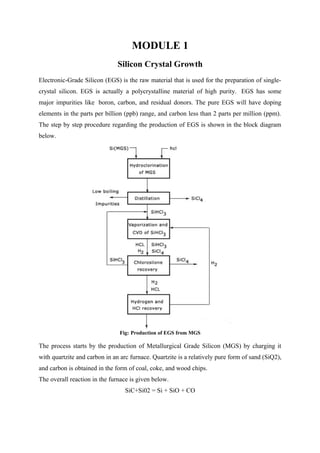
  • 1. MODULE 1 Silicon Crystal Growth Electronic-Grade Silicon (EGS) is the raw material that is used for the preparation of single- crystal silicon. EGS is actually a polycrystalline material of high purity. EGS has some major impurities like boron, carbon, and residual donors. The pure EGS will have doping elements in the parts per billion (ppb) range, and carbon less than 2 parts per million (ppm). The step by step procedure regarding the production of EGS is shown in the block diagram below. Fig: Production of EGS from MGS The process starts by the production of Metallurgical Grade Silicon (MGS) by charging it with quartzite and carbon in an arc furnace. Quartzite is a relatively pure form of sand (SiQ2), and carbon is obtained in the form of coal, coke, and wood chips. The overall reaction in the furnace is given below. SiC+Si02 = Si + SiO + CO
  • 2. VLSI DESIGN The MGS after being drawn off, has to be solidified at a purity of 98%. But this purity is not enough for the manufacture of semiconductor devices. So, the MGS has to be pulverized mechanically and reacted with anhydrous hydrogen chloride (HCI) to form trichlorosilane (SiHCI3). The reaction is shown below. Si + 3HCl = SiHCI3 + H2 With the help of a catalyst, the reaction takes place at a nominal temperature of 300°C. The reaction creates products like silicon tetrachloride (SiCl4) and the chlorides of impurities. At this point the purification process occurs. The purification process has to be done by fractional distillation method as the products trichlorosilane and unwanted chlorides are liquids at room temperature. The purified SiHCI3 is subjected to chemical vapor deposition (CVD). The chemical reaction is a hydrogen reduction of SiHCl3. The chemical reaction is shown below. 2SiHCl3 + 2H2 = 2Si + 6HCl The reaction takes place in a CVD reactor. A resistance heated Si-rod (4-mm diameter), called a slim-rod, is used as the nucleation point for the deposition of silicon. Through the process rods of EGC are obtained. which are up to 0.2 meters (or more) in diameter and several meters in length. EGS can be cut from these rods as single chunks or crushed into nuggets. In order to achieve high overall efficiency, a feedback or recycling of reaction of by-products is done. This is also shown in the figure above. EGS can also be produced by pyrolysis method in which silane (SiH4) will be reacted with heat. The reaction takes place at a high temperature of 900°C. The main advantage of using silane instead of trichlorosilane is the lower production cost and less production of harmful reaction by-products. SiH4 + HEAT = Si + 2H2 In this process the CVD reactor is operated at about 900°C and supplied with silane instead of trichlorosilane. The advantages of producing EGS from silane are lower cost and less harmful reaction by-products. Crystal Structure and Growing The silicon wafermust be single crystal, but it does not represent an ideal crystal due to following reasons: 2
  • 3. VLSI DESIGN ◾The wafer has finite boundaries; thus, atoms at the surfaces are incompletely bonded as against those in the bulk of the wafer material. ◾The atoms are displaced from their ideal locations by thermal agitation. Czochralski Crystal Growth Process (refer written notes) The highly refined silicon (EGS) though free from impurities, is still polycrystalline. Hence it is to be processed to become single crystal. The Czochralski crystal growth process is often used for producing single-crystal silicon ingots. The diagram is given below. Since monolithic ICs are usually fabricated on a substrate which is doped with impurity, the poly-crystalline silicon with an appropriate amount of dopant is-put into a quartz crucible, which is then placed inside a crystal growth furnace. The material is then heated to a temperature that is slightly in excess of the silicon melting pint of 1420 degree Celsius. A small single-crystal rod of silicon called a seed crystal is then dipped into the silicon melt. The conduction of heat up the seed crystal will produce a reduction in the temperature of the melt in contact with the seed crystal to slightly below the silicon melting point. The silicon will therefore freeze onto the end of the seed crystal, and as the seed crystal is slowly pulled up out of the melt it will pull up with it a solidified mass of silicon that will be a 3
  • 4. VLSI DESIGN crystallographic continuation of the seed crystal. Both the seed crystal and the crucible are rotated but in opposite directions during the crystal pulling process in order to produce crystalline ingots of circular cross section. The liquid solid interface remains near to the surface of the melt if the temperature and pulling rate are correctly chosen. Even a long single crystal silicon is pulled from it. The diameter of the ingot is controlled by the pulling rate and the melt temperature, with ingot diameters of about 100 to 150 mm (4 to 6 inches) being the most common. The ingot length will generally be of the order of 3 meter, and several hours are required for the “pulling” of a complete ingot. The crystal pulling is done in an inert-gas atmosphere (usually argon or helium), and sometimes a vacuum is used. This is done to prevent oxidation” The pull-rate is closely related to the heat input and losses, crystal properties and dimensions. The conditions for crystal pulling are therefore carefully controlled. For example, the melt temperature is monitored with a thermocouple and feedback controller. Longer diameter crystals have commercial advantages and can be grown. However, difficulties may be encountered because of resistivity gradient across finished slices. The crystal growth apparatus shown in the figure above consists of the following parts. • Furnace • Crystal pulling mechanism • Ambient control facility • Control system circuitry The furnace consists of a crucible, susceptor (crucible support) and rotational mechanism, heating element and power supply, and a chamber. As the crucible contains the melt, it is the most important component of the growth apparatus. The crucible material should be chemically unreactive with molten silicon. Also, the material should have high melting point, thermal stability, and hardness. The materials for crucible, which satisfy these properties, are silicon nitride (Si3N4) and fused silica (SiO2). The latter is in exclusive use nowadays. Fused silica; however, reacts with silicon, releasing silicon and oxygen into the melt. In tins process the crucible undergoes erosion. The susceptor, is used to support the silica crucible. It also provides for better thermal conditions. Graphite is the material of choice because of its high- temperature properties. The graphite should be pure to prevent contamination of the crystal from impurities that would be volatilized from the graphite at the temperature involved. The susceptor rests on a pedestal whose shaft is connected to a motor that provides rotation. The whole assembly can usually be raised and lowered to keep the melt level equidistant from a 4
  • 5. VLSI DESIGN fixed reference point, which is needed for automatic diameter control. The chamber housing the furnace must provide easy access to the furnace components to facilitate maintenance and cleaning. The furnace structure must be airtight to prevent contamination from the atmosphere, and have a specific design that does not allow any part of the chamber to become so hot that its vapour pressure would be a factor in contaminating the crystal. Hottest parts of the apparatus are water cooled Insulation is usually provided between the heater and the chamber wall. The crystal-pulling mechanism consists of seed shaft or chain, rotation mechanism, and seed chuck. The mechanism controls two parameters of die growth process: pull rate and crystal rotation. Also, the pulling mechanism must have minimum vibration and great precision. The seed holder and pulling mechanism must maintain precise orientation perpendicular to the melt surface. From the figure shown above you can see that the crystal leaves the furnace through a purge tube, where ambient gas, if present, is directed along the surface of the crystal to cool it. From the purge tube, the crystal enters an upper chamber, which is usually separated from the furnace by an isolation valve. The ambient control for the crystal growth apparatus consists of gas source, flow control, purge lube, and exhaust or vacuum system. The crystal growth must be conducted in an inert gas or vacuum as staled earlier. This is necessary because • The hot graphite parts must be protected from oxygen to prevent erosion and • The gas around the process should not react with the molten silicon. Growth in vacuum meets these requirements. Growth in a gaseous atmosphere, generally used on large growers, must use an inert gas such as helium or argon. The inert gas may be at atmospheric pressure or at reduced pressure. The control system for crystal growing may consist of micro processing sensors, and outputs and provides control of process parameters such as temperature, crystal diameter, pull rate and rotation speed. The use of digital or microprocessor-based systems for control is more common because these rely less on operator intervention and have many parts of the process pre-programmed. Silicon Wafer Preparation Ingot Trimming and Slicing As soon as the crystal ingot is obtained using the above processes, the extreme top and bottom portions of the ingot are cut off and the ingot surface is grounded to produce a 5
  • 6. VLSI DESIGN constant and exact diameter. The normal diameter is usually 100,125, or 150 mm. A crystallographic orientation flat is also ground along the length of the ingot. The ingot is then sliced using a large-diameter stainless steel saw blade with industrial diamonds embedded into the inner-diameter cutting edge. This will help in producing circular slices or wafers that are about 600 to 1000 micro meters thick. The orientation flat serves as a useful reference plane for various device processes. Wafer Polishing and Cleaning When the wafer is sliced, its surface will be heavily damaged. This can be made normal only by polishing. The reasons for polishing are given below. • To remove the damaged silicon from the sawn surface. • To produce a highly planar or flat surface that will be required for the photo- lithographic process especially when flue-line geometries are involved. • To improve the parallel. The sliced wafer will have saw marks and is 0.6 to 1 mm thick. This is quite rough. Hence it has to be lapped to produce a flat surface. The wafer, before polishing, may have a surface damage in the order of 75 micro meters. Even through lapping, only 60 micro meters can be polished and scraped. The remaining 15 micro meters has to be removed with the help of etching process. The chemical etch consists of an acid mixture, including nitric acid to oxidize the surface and hydrofluoric acid to dissolve the oxide. The wafer is then made into a mirror like finish by polishing it. This polishing is carried out by using aluminium abrasive powders of decreasing grit size (down to a final 1 micro meters diameter). Even after the polishing, the wafer will still have a surface damage of around 2 micro meters deep. This is removed by an additional chemical etching stage, which can sometimes be simultaneous with the final polishing stage. In most cases, only one side of the wafer s carefully polished to produce a mirror like image. The other side is given a normal lapping procedure to provide a somewhat flat surface with agreeable parallelism. After the wafer polishing operations are completed, the wafers are thoroughly cleaned, and dried, and they are now ready to be used for the various processing steps described in the following sections. Before discussing these steps let us discuss some processing considerations necessary to maintain the purity and perfection of the material. Wafer Processing Considerations 1. Chemical Cleaning 6
  • 7. VLSI DESIGN The wafers are cleaned thoroughly as soon as the polishing is completed. Originally, the silicon wafers are cleaned so as to remove all organic films, heavy metals, and particulars:. The commonly used cleaning agents are aqueous mixtures of NH4OH – H2O2, HCI – H2O2,and,H2SO4-H2O2. All of the above solutions are good enough in removing metallic impurities, but, out of the lot, the HCI – H2O2, mixture is the best 2. Gettering Treatments The transition group elements which act as the metallic impurities are located at the interstitial or substitutional lattice sites and act as generation-recombination centres for the carriers. The precipitated forms of these impurities are usually silicides. These silicides are known to be electrically conductive . In the case of VLSI circuits, these transition group elements decrease their performance, especially in the case of dynamic random access memories and narrow-base bipolar transistors, as they are sensitive to conductive impurity precipitates. Normally, a process called gettering treatment is carried out to remove the impurities. Gettering is a process that removes,and harms the impurities or defects them from the regions in a wafer where devices are fabricated. Pregettering refers to a gettering treatment provided to silicon wafers that are used for IC processing. When the wafer with sinks are developed for device processing, the impurities are absorbed with the help of pregettering process. The common techniques that are used for gettering treatment are given below: • Common mechanical abrasion methods like lapping and sand blasting are carried out to damage the back surface of the wafer. • A focused heat beam from a Q-pulsed, Nd-YAG laser is used to damage the wafer. Dislocations are made in the wafer by rastering the laser beam along the wafer’s back surface. Thus they become favorable trapping sites for fast-diffusing species. • Intrinsic gettering - As told earlier, when an impurity oxygen precipitates, defects are generated. The defects generated by oxygen precipitation are useful as trapping sites. As the wafer is needed for device fabrication, high temperature cycle is employed to lower the oxygen content near the surface of the wafer. Additional thermal cycles are added to promote the formation of oxygen precipitates and defects in the interior of the wafer. Diffusion of Dopant Impurities 7
  • 8. VLSI DESIGN The process of junction formation, that is transition from p to n type or vice versa, is typically accomplished by the process of diffusing the appropriate dopant impurities in a high temperature furnace. Impurity atoms are introduced onto the surface of a silicon wafer and diffuse into the lattice because of their tendency to move from regions of high to low concentration. Diffusion of impurity atoms into silicon crystal takes place only at elevated temperature, typically 900 to 1100°C. Although these are rather high temperatures, they are still well below the melting point of silicon, which is at 1420°C. The rate at which the various impurities diffuse into silicon will be of the order of 1 micro meter per hour at a temperature range stated above, and the penetration depth that are involved in most diffusion processes will be of the order of 0.3 to 30 micro meter. At room temperature the diffusion process will be so extremely slow such that the impurities can be considered to be essentially frozen in place. A method of p-n junction formation which was popular in the early days is the grown junction technique. In this method the dopant is abruptly changed in the melt during the process of crystal growth. A convenient technique for making p-n junction is the alloying of a metal containing doping atoms on a semiconductor with the opposite type of dopant. This is called the alloyed junction technique. The p-n junction using epitaxial growth is widely used in ICs. An epitaxial grown junction is a sharp junction. In terms of volume of production, the most common technique for forming p-n junctions is the impurity diffusion process. This produces diffused junction. Along with diffusion process the use of selective masking to control junction geometry, makes possible the wide variety of devices available in the form of IC’s. Selective diffusion is an important technique in its controllability, accuracy and versatility. Nature of Impurity Diffusion The diffusion of impurities into a solid is basically the same type of process as occurs when excess carriers are created non-uniformly in a semiconductor which cause carrier gradient. In each case, the diffusion is a result of random motion, and particles diffuse in the direction of decreasing concentration gradient The random motion of impurity atoms in a solid is, of course, rather limited unless the temperature is high. Thus diffusion of doping impurities into silicon is accomplished at high temperature as stated above. There are mainly two types of physical mechanisms by which the impurities can diffuse into the lattice. They are 1. Substitutional Diffusion 8
  • 9. VLSI DESIGN At high temperature many atoms in the semiconductor move out of their lattice site, leaving vacancies into which impurity atoms can move. The impurities, thus, diffuse by this type of vacancy motion and occupy lattice position in the crystal after it is cooled. Thus, substitutional diffusion takes place by replacing the silicon atoms of parent crystal by impurity atom. In other words, impurity atoms diffuse by moving from a lattice site to a neighbouring one by substituting for a silicon atom which has vacated a usually occupied site as shown in the figure below. Substitutional diffusion mechanism is applicable to the most common diffusants, such as boron, phosphorus, and arsenic. These dopants atoms are too big to fit into the interstices or voids, so the only way they can enter the silicon crystal is to substitute for a Si atom. In order for such an impurity atom to move to a neighbouring vacant site, it has to overcome energy barrier which is due to the breaking of covalent bonds. The probability of its having enough thermal energy to do this is proportional to an exponential function of temperature. Also, whether it is able to move is also dependent on the availability of a vacant neighbouring site and since an adjacent site is vacated by a Si atom due to thermal fluctuation of the lattice, the probability of such an event is again an exponent of temperature. The jump rate of impurity atoms at ordinary temperatures is very slow, for example about 1 jump per 1050 years at room temperature! However, the diffusion rate can be speeded up by an increase in temperature. At a temperature of the order 1000 degree Celsius, substitutional diffusion of impurities is practically realized in sensible time scales. 2. Interstitial Diffusion In such, diffusion type, the impurity atom does not replace the silicon atom, but instead moves into the interstitial voids in the lattice. The main types of impurities diffusing by such 9
  • 10. VLSI DESIGN mechanism are Gold, copper, and nickel. Gold, particularly, is introduced into silicon to reduce carrier life time and hence useful to increase speed at digital IC’s. Because of the large size of such metal atoms, they do not usually substitute in the silicon lattice. To understand interstitial diffusion, let us consider a unit cell of the diamond lattice of the silicon which has five interstitial voids. Each of the voids is big enough to contain an impurity atom. An impurity atom located in one such void can move to a neighbouring void, as shown in the figure below. In doing so it again has to surmount a potential barrier due to the lattice, this time, most neighbouring interstitial sites are vacant so the frequency of movement is reduced. Again, the diffusion rate due to this process is very slow at room temperature but becomes practically acceptable at normal operating temperature of around 1000 degree Celsius. It will be noticed that the diffusion rate due to interstitial movement is much greater than for substitutional movement. This is possible because interstitial diffusants can fit in the voids between silicon atoms. For example, lithium acts as a donor impurity in silicon, it is not normally used because it will still move around even at temperatures near room temperature, and thus will not be frozen in place. This is true of most other interstitial diffusions, so long-term device stability cannot be assured with this type of impurity. Fick’s Laws of Diffusion The diffusion rate of impurities into semiconductor lattice depends on the following • Mechanism of diffusion • Temperature • Physical properties of impurity • The properties of the lattice environment 10
  • 11. VLSI DESIGN • The concentration gradient of impurities • The geometry of the parent semiconductor The behaviour of diffusion particles is governed by Fick’s Law, which when solved for appropriate boundary conditions, gives rise to various dopant distributions, called profiles which are approximated during actual diffusion processes. In 1855, Fick drew analogy between material transfer in a solution and heat transfer by conduction. Fick assumed that in a dilute liquid or gaseous solution, in the absence of convection, the transfer of solute atoms per unit area in a one-dimensional flow can be described by the following equation F = -D ∂N(x,t)/∂x = -∂F(x,t)/∂x where F is the rate of transfer of solute atoms per unit area of the diffusion flux density (atoms/cm2 -sec). N is the concentration of solute atoms (number of atoms per unit volume/cm3 ), and x is the direction of solute flow. (Here N is assumed to be a function of x and t only), t is the diffusion time, and D is the diffusion constant (also referred to as diffusion coefficient or diffusivity) and has units of cm2 /sec. The above equation is called Fick’s First law of diffusion and states that the local rate of transfer (local diffusion rate) of solute per unit area per unit time is proportional to the concentration gradient of the solute, and defines the proportionality constant as the diffusion constant of the solute. The negative sign appears due to opposite direction of matter flow and concentration gradient. That is, the matter flows in the direction of decreasing solute concentration. Fick’s first law is applicable to dopant impurities used in silicon. In general the dopant impurities are not charged, nor do they move in an electric field, so the usual drift mobility term (as applied to electrons and holes under the influence of electric field) associated with the above equation can be omitted. In this equation N is in general function of x, y, z and t. The change of solute concentration with time must be the same as the local decrease of the diffusion flux, in the absence of a source or a sink. This follows from the law of conservation of matter. Therefore we can write down the following equation ∂N(x,t)/∂t = -∂F(x,t)/∂x Substituting the above equation to ‘F’. We get ∂N(x,t)/∂t = ∂/∂x[D*∂N(x,t)/∂x] When the concentration of the solute is low, the diffusion constant at a given temperature can be considered as a constant. Thus the equation becomes, 11
  • 12. VLSI DESIGN ∂N(x,t)/∂t = D[∂2 N(x,t)/∂x2 ] This is Ficks second law of distribution. Diffusion Profiles Depending on boundary equations the Ficks Law has two types of solutions. These solutions provide two types of impurity distribution namely constant source distribution following complimentary error function (erfc) and limited source distribution following Gaussian distribution function. 1)Constant Source (erfc) Distribution In this impurity distribution, the impurity concentration at the semiconductor surface is maintained at a constant level throughout the diffusion cycle. That is, N (o,t) = NS = Constant The solution to the diffusion equation which is applicable in this situation is most easily obtained by first considering diffusion inside a material in which the initial concentration changes in same plane as x=0, from NS to 0. Thus the equation can be written as N (o,t) = NS = Constant and N(x,t) = 0 Shown below is a graph of the complementary error function for a range of values of its argument. The change in concentration of impurities with time, as described by the equation is also shown in the figure below. The surface concentration is always held at NS, falling to some lower value away from the surface. If a sufficiently long time is allowed to elapse, it is possible for the entire slice to acquire a dopant level of NS per m3 . 12
  • 13. VLSI DESIGN If the diffused impurity type is different from the resistivity type of the substrate material, a junction is formed at the points where the diffused impurity concentration is equal to the background concentration already present in the substrate. In the fabrication of monolithic IC’s, constant source diffusion is commonly used for the isolation and the emitter diffusion because it maintains a high surface concentration by a continuous introduction of dopant. There is an upper limit to the concentration of any impurity that can be accommodated at the semiconductor wafer at some temperature. This maximum concentration which determines the surface concentration in constant source diffusion is called the solid solubility of the impurity. 2)Limited Source Diffusion or Gaussian Diffusion Here a predetermined amount of impurity is introduced into the crystal unlike constant source diffusion. The diffusion takes place in two steps. 1. Predeposition Step – In this step a fixed number of impurity atoms are deposited on the silicon wafer during s short time. 2. Drive-in step – Here the impurity source is turned off and the amounts of impurities already deposited during the first step are allowed to diffuse into silicon water. The essential difference between the two types of diffusion techniques is that the surface concentration is held constant for error function diffusion. It decays with time for the Gaussian type owing to a fixed available doping concentration Q. For the case of modelling the depletion layer of a p-n junction, the erfc is modelled as a step junction and the Gaussian 13
  • 14. VLSI DESIGN as a linear graded junction. In the case of the erfc, the surface concentration is constant, typically the maximum solute concentration at that temperature or solid solubility limit. Parameters which affect diffusion profile • Solid Solubility – In deciding which of the availability impurities can be used, it is essential to know if the number of atoms per unit volume required by the specific profile is less than the diffusant solid solubility. • Diffusion temperature – Higher temperatures give more thermal energy and thus higher velocities, to the diffused impurities. It is found that the diffusion coefficient critically depends upon temperature. Therefore, the temperature profile of diffusion furnace must have higher tolerance of temperature variation over its entire area. • Diffusion time – Increases of diffusion time, t, or diffusion coefficient D have similar effects on junction depth as can be seen from the equations of limited and constant source diffusions. For Gaussian distribution, the net concentration will decrease due to impurity compensation, and can approach zero with increasing diffusion tunes. For constant source diffusion, the net Impurity concentration on the diffused side of the p-n junction shows a steady increase with time. • Surface cleanliness and defects in silicon crystal - The silicon surface must be prevented against contaminants during diffusion which may interfere seriously with the uniformity of the diffusion profile. The crystal defects such as dislocation or stacking faults may produce localized impurity concentration. This results in the degradation of junction characteristics. Hence silicon crystal must be highly perfect. Basic Properties of the Diffusion Process Following properties could be considered for designing and laying out ICs. • When calculating the total effective diffusion time for given impurity profile, one must consider the effects of subsequent diffusion cycles. • The erfc and Gaussian functions show that the diffusion profiles are functions of (x/ √Dt). Hence, for a given surface and background concentration, the junction depth x1 and x2 associated with the two separate diffusions having different times and temperature • Lateral Diffusion Effects – The diffusions proceed sideways from a diffusion window as well as downward. In both types of distribution function, the side diffusion is about 75 to 80 per cent of the vertical diffusion. Dopants and their Characteristics 14
  • 15. VLSI DESIGN The dopants selection affects IC characteristics. Boron and phosphorus are the basic dopants of most ICs. Arsenic and antimony, which are highly soluble in silicon and diffuse slowly, are used before epitaxial processing or as a second diffusion. Gold and silver diffuse rapidly. They act as recombination centres and thus reduce carrier life time. Boron is almost an exclusive choice as an acceptor impurity in silicon since other p-type impurities have limitations as follows : Gallium has relatively large diffusion coefficient in Si02, and the usual oxide window- opening technique for locating diffusion would be inoperative, Indium is of little interest because of its high acceptor level of 0.16 eV, compared with 0.01 eV for boron, which indicates that not all such acceptors would be ionized at room temperature to produce a hole. Aluminium reacts strongly with any oxygen that is present in the silicon lattice. The choice of a particular n-type dopant is not so limited as for p-type materials. The n-type impurities, such as phosphorus, antimony and arsenic, can be used at different stages of IC processing. The diffusion constant of phosphorus is much greater than for Sb and As, being comparable to that for boron, which leads to economies resulting from shorter diffusion times. Dopants in VLSI Technology The common dopants in VLSI circuit fabrication are boron, phosphorus. and arsenic. Phosphorus is useful not only as an emitter and base dopant, but also far gettering fast- diffusing metallic contaminants, such as Cu and An, which cause junction leakage current problems. Thus, phosphorus is indispensable in VLSI technology. However, n-p-n transistors made with arsenic-diffused emitters have better low-current gain characteristics and better control of narrow base widths than those made with phosphorus-diffused emitters. Therefore, in V LSI, the use of phosphorus as an active dopant in small, shallow junctions and low- temperature processing will be limited to its use as the base dopant of p-n-p device and as a gettering agent. Arsenic is the most frequently used dopant for the source and drain regions in n-channel MOSFETs. Diffusion Systems Impurities are diffused from their compound sources as mentioned above. The method impurity delivery to wafer is determined by the nature of impurity source; Two-step diffusion is widely technique. Using this technique, the impurity concentration and profiles can be 15
  • 16. VLSI DESIGN carefully controlled. The type of impurity distribution (erfc or Gaussian) is determined by the choice of operating conditions. The two-step diffusion consists of a deposition step and a drive-in step. In the former step a constant source diffusion is carried out for a short time, usually at a relatively low temperatures, say, 1000°C. In the latter step, the impurity supply is shutoff and the existing dopant is allowed to diffuse into the body of the semiconductor, which is now held at a different temperature, say 1200°C, in an oxidizing atmosphere. The oxide layer which forms on tire surface of the wafer during this step prevents further impurities from entering, or those already deposited, from diffusing out. The final impurity profile is a function of diffusion condition, such as temperature, time, and diffusion coefficients, for each step. • Diffusion Furnace For the various types of diffusion (and also oxidation) processes a resistance-heated tube furnace is usually used. A tube furnace has a long (about 2 to 3 meters) hollow opening into which a quartz tube about 100,150 mm in diameter is placed as shown in the figure below. Diffusion Furnace The temperature of the furnace is kept about1000°C. The temperature within the quartz furnace tube can be controlled very accurately such that a temperature within 1/2°C of the set-point temperature can be maintained uniformly over a “hot zone” about 1 m in length. This is achieved by three individually controlled adjacent resistance elements. The silicon wafers to be processed are stacked up vertically into slots in a quartz carrier or “boat” and inserted into the furnace lube. Diffusion Of p-Type Impurity Boron is an almost exclusive choice as an acceptor impurity in silicon. It has a moderate diffusion coefficient, typically of order I0-16 m2/sec at 1150°C which is convenient for precisely controlled diffusion. It has a solid solubility limit of around 5 x 1026 atoms/m3, so 16
  • 17. VLSI DESIGN that surface concentration can be widely varied, but most reproducible results are obtained when the concentration is approximately 1024/m3, which is typical for transistor base diffusions. • Boron Diffusion using B2H6 (Diborane) Source This is a gaseous source for boron. This can be directly introduced into the diffusion furnace. A number of other gases are metered into the furnace. The principal gas flow in the furnace will be nitrogen (N2) which acts as a relatively inert gas and is used as a carrier gas to be a dilutent for the other more reactive gases. The N2, carrier gas will generally make up some 90 to 99 percent of the total gas flow. A small amount of oxygen and very small amount of a source of boron will make up the rest of the gas flow. This is shown in the figure below. The following reactions will be occurring simultaneously at the surface of the silicon wafers: Si + 02 = SiO2 (silica glass) 2B2H6 + 302 = B2O3 (boron glass) + 6H2 This process is the chemical vapour deposition (CVD) of a glassy layer on (lie silicon surface which is a mixture of silica glass (Si02) and boron glass (B203) is called borosilica glass (BSG). The BSG glassy layer, shown in the figure below, is a viscous liquid at the diffusion temperatures and the boron atoms can move around relatively easily. Diffusion Of Dopants Furthermore, the boron concentration in the BSG is such that the silicon surface will be saturated with boron at the solid solubility limit throughout the time of the diffusion process as long as BSG remains present. This is constant source (erfc) diffusion. It is often called 17
  • 18. VLSI DESIGN deposition diffusion. This diffusion step is referred as pre-deposition step in which the dopant atoms deposit into the surface regions (say 0.3 micro meters depth) of the silicon wafers. The BSG is preferable because it protects the silicon atoms from pitting or evaporating and acts as a “getter” for undesirable impurities in the silicon. It is etched off before next diffusion as discussed below. The pre-deposition step, is followed by a second diffusion process in which the external dopant source (BSG) is removed such that no additional dopants cuter the silicon. During this diffusion process the dopants that are already in the silicon move further in and are thus redistributed. The junction depth increases, and at the same time the surface concentration decreases. This type of diffusion is called drive-in, or redistribution, or limited-source (Gaussian diffusion). • Boron Diffusion using BBr3i (Boron Tribromide) Source This is a liquid source of boron. In this case a controlled flow of carrier gas (N2,) is bubbled through boron tribromide, as shown in the figure below, which with oxygen again produces boron trioxide (BSG) at the surface of the wafers as per following reaction : 4BBr3 + 302 = B203 + 2Br2 Diffusion of n-Type Impurity For phosphorus diffusion such compounds as PH3 (phosphine) and POCl3 (phosphorus oxychloride) can be used. In the case of a diffusion using PoCI3, the reactions occurring at the silicon wafer surfaces will be: Si + 02 = SiO2 (silica glass) 4POCl + 302 = 2P205 + 6Cl2 This will result in the production of a glassy layer on the silicon wafers (hat is a mixture of phosphorus glass and silica glass called phosphorosilica glass (PSG), which is a viscous liquid at the diffusion temperatures. The mobility of the phosphorus atoms in this glassy layer and the phosphorus concentration is such that the phosphorus concentration at the silicon surface will be maintained at the solid solubility limit throughout the time of the diffusion process (similar processes occur with other dopants, such as the case of arsenic, in winch arsenosilica glass is formed on the silicon surface. The rest of the process for phosphorus diffusion is similar to boron diffusion, that is, after deposition step, drive-in diffusion is carried out. 18
  • 19. VLSI DESIGN P205 is a solid source for phosphorus impurity and can be used in place of POCl3. However POCl3 offers certain advantages overP205 such as easier source handling, simple furnace requirements, similar glassware for low and high surface concentrations and better control of impurity density from wafer to wafer and from run to run. Ion Implantation Ion Implantation is an alternative to a deposition diffusion and is used to produce a shallow surface region of dopant atoms deposited into a silicon wafer. This technology has made significant roads into diffusion technology in several areas. In this process a beam of impurity ions is accelerated to kinetic energies in the range of several tens of kV and is directed to the surface of the silicon. As the impurity atoms enter the crystal, they give up their energy to the lattice in collisions and finally come to rest at some average penetration depth, called the projected range expressed in micro meters. Depending on the impurity and its implantation energy, the range in a given semiconductor may vary from a few hundred angstroms to about 1micro meter. Typical distribution of impurity along the projected range is approximately Gaussian. By performing several implantations at different energies, it is possible to synthesize a desired impurity distribution, for example a uniformly doped region. Ion Implantation System A typical ion-implantation system is shown in the figure below. 19
  • 20. VLSI DESIGN A gas containing the desired impurity is ionized within the ion source. The ions are generated and repelled from their source in a diverging beam that is focussed before if passes through a mass separator that directs only the ions of the desired species through a narrow aperture. A second lens focuses this resolved beam which then passes through an accelerator that brings the ions to their required energy before they strike the target and become implanted in the exposed areas of the silicon wafers. The accelerating voltages may be from 20 kV to as much as 250 kV. In some ion implanters, the mass separation occurs after the ions are accelerated to high energy. Because the ion beam is small, means are provided for scanning it uniformly across the wafers. For this purpose the focussed ion beam is scanned electrostatically over the surface of the wafer in the target chamber. Repetitive scanning in a raster pattern provides exceptionally uniform doping of the wafer surface. The target chamber commonly includes automatic wafer handling facilities to speed up the process of implanting many wafers per hour. Properties of Ion Implantation The depth of penetration of any particular type of ion will increase with increasing accelerating voltage. The penetration depth will generally be in the range of 0.1 to 1.0 micro meters. Annealing after Implantation After the ions have been implanted they are lodged principally in interstitial positions in the silicon crystal structure, and the surface region into which the implantation has taken place 20
  • 21. VLSI DESIGN will be heavily damaged by the impact of the high-energy ions. The disarray of silicon atoms in the surface region is often to the extent that this region is no longer crystalline in structure, but rather amorphous. To restore this surface region back to a well-ordered crystalline state and to allow the implanted ions to go into substitutional sites in the crystal structure, the wafer must be subjected to an annealing process. The annealing process usually involves the heating of the wafers to some elevated temperature often in the range of 1000°C for a suitable length of time such as 30 minutes. Laser beam and electron-beam annealing are also employed. In such annealing techniques only the surface region of the wafer is heated and re-crystallized. An ion implantation process is often followed by a conventional-type drive-in diffusion, in which case the annealing process will occur as part of the drive-in diffusion. Ion implantation is a substantially more expensive process than conventional deposition diffusion, both in terms of the cost of the equipment and the throughput, it does, however, offer following advantages. Advantages of Ion Implantation • Ion implantation provides much more precise control over the density of dopants deposited into the wafer, and hence the sheet resistance. This is possible because both the accelerating voltage and the ion beam current are electrically controlled outside of the apparatus in which the implants occur. Also since the beam current can be measured accurately during implantation, a precise quantity of impurity can be introduced. Tins control over doping level, along with the uniformity of the implant over the wafer surface, make ion implantation attractive for the IC fabrication, since this causes significant improvement in the quality of an IC. • Due to precise control over doping concentration, it is possible to have very low values of dosage so that very large values of sheet resistance can be obtained. These high sheet resistance values are useful for obtaining large-value resistors for ICs. Very low-dosage, low-energy implantations are also used for the adjustment of the threshold voltage of MOSFET’s and other applications. • An obvious advantage of implantation is that it can be done at relatively low temperatures, this means that doped layers can be implanted without disturbing previously diffused regions. This means a lesser tendency for lateral spreading. High-Current High-Energy Implantation Machines 21
  • 22. VLSI DESIGN The ion-implantation apparatus, discussed above, has limits to energy range. The minimum implantation energy is usually set by the extraction voltage, that is, the voltage causing the ions to move out of the ion source into the mass separator. This voltage (which is typically 20 KeV) cannot be reduced too far without drastically reducing beam current. The maximum implantation energy is set by the design of the high voltage equipment. The only way to circumvent this is to implant multiply-charged ions. High beam currents are obtained by using multiple extraction electrodes and higher voltages. To get a final beam of suitable energy a combination of acceleration and deceleration modes of operation is used. The electrostatic scanning is not suitable for high-beam currents, as it disrupts space charge neutrality and leads to beam “blow-up”. Therefore a mechanical scanning system is usually used. In this case, the wafer is scanned past a stationary beam. This method has the added advantage of keeping the same beam angle across the whole wafer, whereas an electrostatic system can vary by ±2° for 100 mm wafers. However, mechanical scanning puts new requirements on the wafer holder. High-energy implantation, at MeV energies, makes possible several new processing techniques required for VLSI. High-energy implantation machines however introduce high-voltage breakdown problem. At about 400 KeV of energy electrical breakdown of the air around the high voltage equipment occurs. Hence, above 400 KeV, conventional equipment is used. Also, high energy implants frequently require water stages heated up to 600 degree Celsius, so that self annealing during implantation minimizes damage in the surface layer. Mechanical scanning is used because of the difficulty of electrostatically scanning a high-energy beam. Problems in VLSI Processing Now a day’s large diameter wafers are feasible. Large size wafers are necessary for VLSI. This makes the task of uniformly implanting a wafer increasingly difficult. This in turn has effect on sheet resistance. Ion implantation is basically clean process because contaminant ions are separated from the beam before they hit the target. There are still several sources of contamination possible near the end of the beam line, which can result in contaminant dose up to 10 percent of the intended ion dose, for example, metal atoms knocked from chamber walls, water holder, masking aperature and so on. Annealing, as discussed earlier, is required to repair lattice damage and put dopant atoms on substitutional site where they will be electrically active. The success of 22
  • 23. VLSI DESIGN annealing is often measured in terms of the fraction of the dopant that is electrically active, as found experimentally using a Hall Effect technique. For VLSI, the challenge in annealing is not simply to repair damage and activate dopant, but to do so while minimizing diffusion so that shallow implants remain shallow. This has motivated much work in rapid thermal annealing (RTA), where annealing times are on the order of seconds. RTA uses tungsten-halogen lamps or graphite resistive strips to heat the wafer from one or both sides as against conventional furnace annealing where times or on the order of minutes. Modern device structures, such as the lightly-doped drains (LDD) for MOSFET, require precise control of dopant distribution vertically and lateral on a very fine scale. For VLSI CMOS structure, we need to form shallow n and layers with implantation energies within the reach of standard machines. As stated earlier, the ion velocity, perpendicular to the surface, determines the projected range of an implanted ion distribution. If the water is tilted at a large angle to the ion beam then the effective ion energy is greatly reduced tilted ion beams, thus, make it possible to achieve extremely shallow dopant distributions using comparatively high implantation energies. We can circumvent the problem of implanting a shallow layer in silicon completely if instead we implant entirely into a surface layer and then diffuse the dopant into the substrate. This is most often done when the surface film is to be used as a conductor making contact to the substrate. Diffusion results in steep dopant profiles without damage to the silicon lattice. Dopant diffusion in silicides and polysilicon is generally much faster than in single-crystal silicon, so the implanted atoms soon become uniformly distributed in the film. Importance of Ion Implantation for VLSI Technology Ion implantation is a very popular process for VLSI because it provides more precise control of dopants (as compared to diffusion). With the reduction of device sizes to the submicron range, the electrical activation of ion-implanted species relies on a rapid thermal annealing technique, resulting in as little movement of impurity atoms as possible. Thus, diffusion process has become less important than methods for introducing impurity atoms into silicon for forming very shallow junctions, an important feature of VLSI circuits. Ion, implantation permits introduction of the dopant in silicon that is controllable, reproducible and free from undesirable side effects. Over 23
  • 24. VLSI DESIGN Oxidation The function of a layer of silicon dioxide (SiO2) on a chip is multipurpose. SiO2 plays an important role in IC technology because no other semiconductor material has a native oxide which is able to achieve all the properties of SiO2. The role of SiO2 in IC fabrication is as below • It acts as a diffusion mask permitting selective diffusions into silicon wafer through the window etched into oxide. • It is used for surface passivation which is nothing but creating protective SiO2 layer on the wafer surface. It protects the junction from moisture and other atmospheric contaminants. • It serves as an insulator on the water surface. Its high relative dielectric constant, which enables metal line to pass over the active silicon regions. • SiO2 acts as the active gate electrode in MOS device structure. • It is used to isolate one device from another. • It provides electrical isolation of multilevel metallization used in VLSI. It is fortunate that silicon has an easily formed protective oxide, for otherwise we should have to depend upon deposited insulators for surface protection. Since SiO2 produces a stable layer, this has held back germanium IC technology. Growth and Properties of Oxide Layers on Silicon Silicon dioxide (silica) layer is formed on the surface of a silicon wafer by thermal oxidation at high temperatures in a stream of oxygen. Si+02 = SiO2 (solid) The oxidation furnace used for this reaction is similar to the diffusion furnace. The thickness of the oxide layer depends on the temperature of the furnace, the length of time that the wafers are in it, and the flow rate of oxygen. The rate of oxidation can be significantly increased by adding water vapour to the oxygen supply to the oxidizing furnace. Si + 2H2O = SiO2 + 2H2 The time and temperature required to produce a particular layer thickness arc obtained from empirically determined design curves, of the type shown in the figures given below corresponding to dry- oxygen atmosphere and also corresponding to steam atmosphere. 24
  • 25. VLSI DESIGN Growth and Properties of Oxide Layers on Silicon In the past, steam was obtained by boiling ultra-high-purity water and passing it into the high- temperature furnace containing the silicon wafers; however, present day technologies generally use hydrogen and oxygen which are ignited in the furnace tube to form the ultra high-purify water vapour. The process of silicon oxidation takes place many times during the fabrication of an IC. Once silicon has been oxidized the further growth of oxide is controlled by the thickness of the initial or existing oxide layer. Kinetics of oxidation A well established model for thermal oxide growth has been proposed by Deal and Grove Concept and Formulation (just for extra information-Not in syllabus) If one assumes that the oxidation process is dominated by the inward movement of the oxidant species, the transported species must go through the following stages: (1) It is transported from the bulk of the oxidizing gas to the outer surface of oxide, where it is adsorbed. (2) It is transported across the oxide film towards silicon. 25
  • 26. VLSI DESIGN (3) It reacts at the interface with silicon and form a new layer of SiO2. Each of these steps can be described as independent flux equation. The adsorption of oxidants is written as (1) where is the gas-phase transport coefficient, is the equilibrium concentration of the oxidants in the surrounding gas atmosphere, and Co is the concentration of oxidants at the oxide surface at any given time. It was found experimentally that wide changes in gas flow rates in the oxidation furnaces, changes in the spacing between wafers on the carrier in the furnace, and a change in wafer orientation (standing up or lying down) cause only little difference in oxidation rates. These results imply that is very large, or that only a small difference between and Co is required to provide the necessary oxidant flux. is also the solubility limit in the oxide, which is assumed to be related to the partial pressure p of the oxidant in the gas atmosphere by Henry's law (2) At natural ambient pressure of 1 atm and at a temperature of 1000 C, the solubility limits are 5.2 x10 cm for O2, and 3.0 x10 cm for H2O. The flux F2 represents the diffusion of the oxidants through the oxide layer to the Si-SiO2 interface, which can be expressed as (3) where is the oxidant diffusivity in the oxide, Cs is the oxidant concentration at the oxide- silicon interface, and xo represents the oxide thickness. In this expression it is assumed that the process is in steady state (no changing rapidly with time), and that there is no loss of oxidants when they diffuse through the oxide. Under these conditions, F2 must be constant through the oxide and hence the derivative can be replaced simply by a constant gradient.The third part of the oxidation process is the flux of oxidants consumed by the oxidation reaction at the oxide-silicon interface given by (4) with ks as the surface rate constant. ks really represents a number of processes occurring at the Si/SiO2 interface. These may include oxidant (O2 2O), Si-Si bond breaking, and/or Si-O 26
  • 27. VLSI DESIGN bond formation. The rate at which this reaction takes place should be proportional to the oxidant concentration at the interface Cs. Figure 2.16: One-dimensional model for the oxidation of silicon. Deal and Grove assumed that in the steady state condition these three fluxes are equal, which allows to express them as (5) The rate of oxide growth is proportional to the flux of oxidant molecules, (6) where N is the number of oxidant molecules incorporated per unit volume. The differential equation can be simplified as (7) with the physically based parameters (8) (9) Growth Rate of Silicon Oxide Layer The initial growth of the oxide is limited by the rate at which the chemical reaction takes place. After the first 100 to 300 A of oxide has been produced, the growth rate of the oxide 27
  • 28. VLSI DESIGN layer will be limited principally by the rate of diffusion of the oxidant (02 or H20) through the oxide layer, as shown in the figures given below. The rate of diffusion of O2 or H2O through the oxide layer will be inversely proportional to the thickness of the layer, so that we will have that dx/dt = C/x where x is the oxide thickness and C is a constant of proportionality. Rearranging this equation gives xdx = Cdt Integrating this equation both sides yields, x2 /2 = Ct Solving for the oxide thickness x gives, x = √2Ct We see that after an initial reaction-rate limited linear growth phase the oxide growth will become diffusion-rate limited with the oxide thickness increasing as the square root of the growth time. This is also shown in the figure below. The rate of oxide growth using H2O as the oxidant will be about four times faster than the rate obtained with O2. This is due to the fact that the H2O molecule is about one-half the size of the O2 molecule, so that the rate of diffusion of H2O through the SiO2 layer will be much greater than the O2 diffusion rate. Oxide Charges The interlace between silicon and silicon dioxide contains a transition region. Various charges are associated with the oxidised silicon, some of which are related to the transition region. A charge at the interface can induce a charge of the opposite polarity in the underlying silicon, thereby affecting the ideal characteristics of the MOS device. This results in both yield and reliability problems. The figure below shows general types of charges. 28
  • 29. VLSI DESIGN • Interface-trapped charges These charges at Si-SiO2 are thought to result from several sources including structural defects related to the oxidation process, metallic impurities, or bond breaking processes. The density of these charges is usually expressed in terms of unit area and energy in the silicon band gap. • Fixed oxide charge This charge (usually positive) is located in the oxide within approximately 30 A of the Si – SiO2 interface. Fixed oxide charge cannot be charged or discharged. From a processing point of view, fixed oxide charge is determined by both temperature and ambient conditions. • Mobile ionic charge This is attributed to alkali ions such as sodium, potassium, and lithium in the oxides as well as to negative ions and heavy metals. The alkali ions are mobile even at room temperature when electric fields are present. • Oxide trapped charge This charge may be positive or negative, due to holes or electrons trapped in the bulk of the oxide. This charge, associated with defects in the Si02, may result from ionizing radiation, avalanche injection. Effect of Impurities on the Oxidation Rate The following impurities affect the oxidation rate 1. Water 2. Sodium 3. Group III and V elements 4. Halogen In addition damage to the silicon also affects oxidation rate. As wet oxidation occurs at a substantially greater rate than dry oxygen, any unintentional moisture accelerates the dry 29
  • 30. VLSI DESIGN oxidation. High concentrations of sodium influence the oxidation rate by changing the bond structure in the oxide, thereby enhancing the diffusion and concentration of the oxygen molecules in the oxide. During thermal oxidation process, an interface is formed, which separates the silicon from silicon dioxide. As oxidation proceeds, this interface advances into the silicon. A doping impurity, which is initially present in the silicon, will redistribute at the interface until its chemical potential is the same on each side of the interface. This redistribution may result in an abrupt change in impurity concentration across the interface. The ratio of the equilibrium concentration of the impurity, that is, dopant in silicon to that in SiO2 at the interface is called the equilibrium segregation coefficient. The redistribution of the dopants at the interface influences the oxidation behaviour. If the dopant segregates into the oxide and remains there (such as Boron, in an oxidizing ambient), the bond structure in the silica weakens. This weakened structure permits an increased incorporation and diffusivity of the oxidizing species through the oxide thus enhancing the oxidation rate. Impurities that segregate into the oxide but then diffuse rapidly through it (such as aluminium, gallium, and indium) have no effect on the oxidation kinetics. Phosphorus impurity shows opposite effect to that of boron, that is, impurity segregation occurs in silicon rather than Si02. The same is true for As and Sb dopants. Halogen (such as chlorine) impurities are intentionally introduced into the oxidation ambient to improve both the oxide and the underlying silicon properties. Oxide improvement occurs because there is a reduction in sodium ion contamination, increase in oxide breakdown strength, and a reduction in interface trap density. Traps arc energy levels in the forbidden energy gap which are associated with defects in the silicon. Growth and Properties of Thin Oxides MOS VLSI technology requires silicon dioxide thickness in the 50 to 500 A range in a repeatable manner. This section is devoted to the growth and properties of such thin oxide. This oxide must exhibit good electrical properties and provide long-term reliability. As an example, the dielectric material for MOS devices can be thin thermal oxide. This dielectric is an active component of the storage capacitor in dynamic RAMs, and its thickness determines the amount of charge that can be stored. The growth of thin oxide must be slow enough to obtain uniformity and reproducibility. Various growth techniques for thin oxide are dry oxidation, dry oxidation with HCl, sequential oxidations using different temperatures and ambients, wet oxidation, reduced pressure techniques, and high pressure/low temperature oxidation. High pressure oxidation is 30
  • 31. VLSI DESIGN discussed later. The oxidation rate will, of course, be lower at lower temperatures and at reduced pressures. Ultra-thin oxide (<50 A) have been produced using hot nitric acid, boiling water, and air at room temperatures. Some recent developments in thin oxide growth technique are (i) Rapid thermal oxidation performed in a controlled oxygen ambient with heating provided by tungsten-halogen lamps and (ii) Ultraviolet pulsed laser excitation in an oxygen environment. The properties of thin oxide depend upon the growth technique employed. For example, oxide density increases as the oxidation temperature is reduced. Additionally, HCl ambients have typically been used to passivate ionic sodium, improve the breakdown voltage, and getter impurities and defects in the silicon. This passivation effect begins to occur only in the higher temperature range. For thin oxides, there is an increase in leakage for a given voltage. In thin oxides the dielectric breakdown may be field-dependent (breakdown in a ramping field) or time- dependent (breakdown at a constant field). This breakdown is a failure mode for MOS ICs. Thinner oxides are more prone to failure. High Pressure Oxidation There is a benefit of increase in the oxidation rate if the thermal oxidation is carried out at pressures that are much above atmospheric pressure. The rate of diffusion of the oxidant molecules through an oxide layer is proportional to the ambient pressure. For example, at a pressure of 10 atm the diffusion rate will be increased by a factor of 10 and the corresponding oxidation time can be reduced by nearly the same factor. Alternatively, the oxidation can be done for the same length of time, but the temperature required will be substantially lower. Thus, one principal benefit of high-pressure oxidation processing is lower-temperature processing. The lower processing temperature reduces the formation of crystalline defects and produces less effect on previous diffusions and other processes. The shorter oxidation time is also advantageous in increasing the system throughput. The major limitation of this process is the high initial cost of the system. Applications Oxide Masking The oxide layer is used to mask an underlying silicon surface against a diffusion (or ion implantation) process. The oxide layer is patterned by the photolithographic process to produce regions where there are opening or “windows” where the oxide has been removal to expose the underlying silicon. Then these exposed silicon regions are subjected to the 31
  • 32. VLSI DESIGN diffusion (or implantation) of dopants, whereas the unexposed silicon regions will be protected. The pattern of dopant that will be deposited into the silicon will thus be a replication of the pattern of opening in the oxide layer. The replication is a key factor in the production of tiny electronic components. The thickness of oxide needed for diffusion masking is a function of the type of diffusant and the diffusion time and temperature conditions. In particular, an oxide thickness of some 5000 A will he vufftcieni to mask against almost all diffusions. This oxide thickness will also be sufficient to block almost alt but the highest-energy ion implantation. Oxide Passivation The other function of Si02 in IC fabrication is the surface passivation. This is nothing but creating protective Si02 layer on the wafer surface. The figure below shows a cross-sectional view of a p-n junction produced by diffusion through an oxide window. There are lateral diffusion effects, that is, the diffusion not only proceeds in the downward direction, but also sideways as well, since diffusion is an isotropic process. The distance from the edge of the oxide window to the junction in the lateral direction underneath die oxide is indicated as yj. Lithography Lithography is the process of transferring geometric shapes on a mask to the surface of a silicon wafer. When a sample of crystalline silicon is covered with silicon dioxide, the oxide- layer acts as a barrier to the diffusion of impurities, so that impurities separated from the surface of the silicon by a layer of oxide do not diffuse into the silicon during high- temperature processing. The selective removal of the oxide in the desired area is performed with lithography. Thus, the areas over which diffusions are effective are defined by the oxide layer with windows cut 32
  • 33. VLSI DESIGN in it, through which diffusion can take place. The windows are produced by the lithographic process. This process is the means by which microscopically small electronic circuits and devices can be produced on silicon wafers resulting in as many as 10000 transistors on a 1 cm x 1 cm chip. In IC fabrication a number of masks are employed. Except for the first mask, every mask must be aligned to the pattern produced by the previous mask. This is done using mask aligner. The mask aligner may be contact type or proximity type or projection type. Accordingly we have three types of printing. They are ◾Contact printing ◾Proximity printing ◾Projection printing Photolithography In this process the exposing radiation, such as ultraviolet (UV) light in case of photolithography, is transmitted through the clear parts of the mask. The circuit pattern of opaque chromium blocks some of die radiation. This type of chromium/glass mask is used with UV light. Photolithographic Process Steps 1. Photoresist Application (Spinning) A drop of light-sensitive liquid called photoresist is applied to the centre of the oxidized silicon wafer that is held down by a vacuum chuck. The wafer is then accelerated rapidly to a rotational velocity in the range 3000 to 7000 RPM for some 30 to 60 seconds. This action spreads the solution in a thin, nearly uniform coat and spins off the excess liquid. The thickness of the coat so obtained is in the range 5000 to 10000 A, as shown in the figure below. The thickness of the photoresist layer will be approximately inversely proportional to the square root of the rotational velocity. Sometimes prior to the application of the photoresist the silicon wafers are given a “bake-out” at a temperature Of at least 100°C to drive off moisture from the wafer surfaces so as to obtain better adhesion of the photoresist. Typical photoresist used is Kodak Thin Film Resist (KTFR). 2. Prebake The silicon wafers coated with photoresist are now put into an oven at about 80°C for about 30 to 60 minutes to drive off solvents in the photoresist and to harden it into a semisolid film. 3. Alignment and Exposure 33
  • 34. VLSI DESIGN The coated wafer, as above, is now placed in an apparatus called a mask aligner in very close proximity (about 25 to 125 micro meters) to a photomask. The relative positions of the wafer and the photomasks are adjusted such that the photomask is correctly lined up with reference marks or a pre-existing pattern on the wafer. The photomask is a glass plate, typically about 125 mm square and about 2 mm thick. The photomask has a photographic emulsion or thin film metal (generally chromium) pattern on one side. The pattern has clear and opaque areas. The alignment of the photomask to the wafer is often required to be accurate to within less than 1 micro meter, and in some cases to within 0.5 micro meters. After proper alignment has been achieved, the wafer is brought into direct contact with the photomask. Photomask making will be described separately. A highly collimated ultraviolet (UV) light is then turned on and the areas of the silicon wafer that are not covered by the opaque areas of the photomask are exposed to ultraviolet radiation, as shown in the figure. The exposure time is generally in the range 3 to 10 seconds and is carefully controlled such that the total UV radiation dosage in watt-seconds or joules is of the required amount. 4. Development Two types of photoresist exist- negative photoresist and positive photoresist. In the present description negative photoresist is used in which the areas of the photoresist that are exposed the ultraviolet radiation become polymerized. The polymerization process increases the length of the organic chain molecules that make up the photoresist. This makes the resist tougher and makes it essentially insoluble in the developer solution. The resisting photoresist pattern after the development process will therefore be a replication of the photomask pattern, with the clear areas on the photomask corresponding to the areas where the photoresist remains on the wafers, as shown in the figure below. An opposite type of process occurs with positive photoresist. Exposure to UV radiation results in depolymerization of the photoresist. This makes these exposed areas of the photoresist readily soluble in the developer solution, whereas the unexposed areas are essentially insoluble. The developer solution will thus remove the exposed or depolymerized regions of the photoresist, whereas the unexposed areas will remain on the wafer. Thus again there is a replication of the photomask pattern, but this time the clear areas of the photomask produce the areas on the wafer from which the photoresist has been removed. 5. Postbake After development and rinsing the wafers are usually given a postbake in an oven at a temperature of about 150°C for about 30 to 60 minutes to toughen further the remaining resist 34
  • 35. VLSI DESIGN on the wafer. This is to make it adhere better to the wafer and to make it more resistant to the hydrofluoric acid [HF] solution used for etching of the silicon dioxide. 6. Oxide Etching The remaining resist is hardened and acts as a convenient mask through which the oxide layer can be etched away to expose areas of semiconductor underneath. These exposed areas are ready for impurity diffusion. For etching of oxide, the wafers are immersed in or sprayed with a hydrofluoric [HF] acid solution. This solution is usually a diluted solution of typically 10: 1, H2O : HF, or more often a 10 : 1 NH4F [ammonium fluoride]: HF solution. The HF solutions will etch the SiO2 but will not attack the underlying silicon, nor will it attack the photoresist layer to any appreciable extent. The wafers are exposed to the etching solution ion enough to remove the SiO2 completely in the areas of the wafer that are not covered by the photoresist as shown in the figure. The duration of oxide etching should be carefully controlled so that all of the oxide present only in the photoresist window is removed. If etching time is excessively prolonged, it will result in more undercutting underneath the photoresist and widening of the oxide opening beyond what is desired. The above oxide etching process is termed wet etching process since the chemical reagents used are in liquid form. A newer process for oxide etching is a dry etching process called plasma etching. Another dry etching process is ion milling. 7. Photoresist Stripping Following oxide etching, the remaining resist is finally removed or stripped off with a mixture of sulphuric acid and hydrogen peroxide and with the help of abrasion process. Finally a step of washing and drying completes the required window in the oxide layer. The figure below shows the silicon wafer ready for next diffusion. 35
  • 36. VLSI DESIGN Photolithographic Process Steps Negative photoresists, as above, are more difficult to remove. Positive photoresists can usually be easily removed in organic solvents such as acetone. The photolithography may employ contact, proximity, or projection printing. For IC production the line width limit of photolithography lies near 0.4 micro meters, although 0.2 micro meters features may be printed under carefully controlled conditions. At present, the photolithography occupies the primary position among various lithographic techniques. Photoresists One of the major factors in providing increasingly complex devices has been improvement in photolithographic art. A large part of this improvement has been due to high quality photoresist, materials as improved techniques of coating, baking, exposing and developing photoresists. The principal constituents of a photoresist solution are a polymer, a sensitizer and a suitable solvent system Polymers have properties of excellent film forming and coating. Polymers generally used are polyvinyl cinnamate, partially cyclized isoprene family and other types are phenol formaldehyde. When photoresist is exposed to light, sensitizer absorbs energy and initiates chemical changes in the resist. The sensitizers are chromophoric organic molecules. They greatly enhance cross linking of the photoresist. Cross linking of polymer or long chain formation of considerable number of monomers makes high molecular weight molecules on exposure to light radiation, termed as photo-polymerization. Typical sensitizers are carbonyl compounds, Benzoin, Benzoyl peroxide, Benzoyl disulphide, nitrogen compounds and halogen compounds. The solvents used to keep the polymers in solution are mixture of organic liquids. They include aliphetic esters such as butyl acetate and cellosolve acetate, aromatic hydrocarbons like xylene and Ethylbenzene, chlorinated hydrocarbons like chlorobenzene and methylene chloride and ketones such as cyclohexanone. The same solvents are used as thinners and developers. Characteristics of Good Photoresist To achieve faithful registration of the mask geometry over the substrate surface, the resist should satisfy following conditions. • Uniform film formation • Good adhesion to the substrate • Resolution 36
  • 37. VLSI DESIGN • Resistance to wet and dry etch processes Types of Photoresist Polymers film is either photosensitive or capable or reacting with the pholysis product of additional compound so that the solubility increases or decreases greatly by exposure to UV (ultra-violet) radiation. According to the changes that take place, photoresists are termed negative or positive. Materials which are rendered less soluble in a developer solution by illumination^ yield a negative pattern of the mask and are called negative photoresists. Conversely, positive photoresists become more soluble when subjected to light and therefore yield a positive image of the mask. Negative Photoresist Kodak negative photoresist contain polyvinyl cinnametes. KPR is being used in printing circuit boards. KTFR is widely used in fabrication of ICs. It provides good adhesion to silicon dioxide and metal surfaces. It gives well etch results to different etchant solutions. For finer resolution, thinner coating of KTFR is used. To achieve controlled and uniform thickness, the viscosity of resist is suitably lowered using thinners. Another negative photoresist is Kodak Microneg 747 which provides high scan speeds at high aperature giving high throughput and resolution. Positive Photoresist Positive Photoresists have solved the problem of resolution and substrate protection. Photo resists can be used at a coating thickness of 1 micro meter that eliminates holes and minimises defects from dust. Positive photoresist is inherently of low solubility (polymerized) material. The base polymer is active by itself. A sensitizer, when absorbs light, makes the base resist soluble in an alkali developer. Positive photoresists are Novolac resins. Typical solvents are cellosolve acetate, butyl acetate, xylene and toluene. Resist requirements for VLSI For fine line geometries in VLSI circuits, the resist requirements become more stringent. The resist properties should meet the required demand of high resolution. Here the resist should exhibit • High sensitivity for partial exposure tool chosen • Dry developing, dry compatibility 37
  • 38. VLSI DESIGN • Vertical profile control Photomask Fabrication Photolithography is used to produce windows in the oxide layer of the silicon wafer, through which diffusion can take place. For this purpose photomask is required. In this section we shall discuss various techniques of mask fabrication. The pattern appearing on the mask is required to be transferred to the wafer. For this purpose various exposure techniques are employed. We will also discuss these techniques. Mask Making IC fabrication is done by the batch processing, where many copies of the same circuit are fabricated on a single wafer and many wafers are fabricated at the same time. The number of wafers processed at one time is called the lot size and many vary between 20 to 200 wafers. Since each IC chip is square and the wafer is circular, the number of chips per wafer is the number of complete squares of a given size that can fit inside a circle. The pattern for the mask is designed from the circuit layout. Many years ago, bread boarding of the circuit was typical. In this, the circuit was actually built and tested with discrete components before its integration. At present, however, when LSI and VLSI circuits contain from a thousand to several hundred thousand components, and switching speeds are of such high order where propagation delay time between devices is significant, bread boarding is obviously not practical. Present-day mask layout is done with the help of computer. The photographic mask determines the location of all windows in the oxide layer, and hence areas over which a particular diffusion step is effective. Each complete mask consists of a photographic plate on which each window is represented by an opaque are, the remainder being transparent. Each complete mask will not only include all the windows for the production of one stage of a particular IC, but in addition, all similar areas for all such circuits on the entire silicon as shown in the figure below. It will be obvious that a different mask is required for each stage in the production of an array of IC’s on a wafer. There is also a vital requirement for precise registration between one mask and the other in series, to ensure that there is no overlap between components, and that each section of a particular transistor is formed in precisely the correct location. To make a mask for one of the production stages, a master is first prepared which is an exact replica of that portion of the final mask associated with one individual integrated circuit, but which is 250x [say] enlargement of the final size of IC. The figure below shows a possible master for the production of a mask to define a particular layer of diffusion for a hypothetical circuit. Art work at enlarge size avoids large tolerance errors. Large size also permits the art 38
  • 39. VLSI DESIGN work to be dealt easily by human operator. In the design of the art work, the locations of all components that is, resistor, capacitor, diode, transistor and so on, are determined on the surface of the chip. Therefore, six or more layout drawings are required. Each drawing shows the position of Windows that are required for a particular step of the fabrication. For complex circuit the layout is generated by the use of computer-aided graphics. Photomask Fabrication The master, typically of order 1 m x 1 m, is prepared from cut and strip plastic material which consists of two plastic films, one photographically opaque called Rubilith and the other transparent [mylar], which are laminated together. The outline of the pattern required is cut in the red coating of Rubilith (which is opaque) using a machine controlled cutter on an illuminated drafting table. The opaque film is then peeled off to reveal transparent areas, each representing a window region in die final mask. The next step is to photograph the master using back illumination, to produce a 25 x reduced sub-master plate. This plate is used in a step and repeat camera which serves the dual purpose of reducing the pattern by a further 10 x to finished size and is also capable of being stepped mechanically to produce an array of identical patterns on the final master mask, each member of the many corresponding to one complete IC. Instead of the photographic plate being transported mechanically in discrete steps, better accuracy may be achieved by using continuous plate movement; discrete exposures then being made by an electronically synchronized flash lamp which effectively freezes the motion. 39
  • 40. VLSI DESIGN The entire sequence just described can be done with plates containing a photosensitive emulsion; typically the emulsion is considered too vulnerable to abrasion and tears. For this reason, masks are often made of harder materials such as chrome or iron oxide. For very complex circuits automated mask generation equipment is used. In this, a computer controlled light flashes to build up the pattern on a photographic film by a series of line or block exposures, the resulting film is then reduced and handled in a step and repeat system to create the production mask. Alternatively, the master mask can be generated by an electron beam exposure system, again controlled by computer. Various Printing Techniques Photolithography comprises the formation of images with visible or U V radiation in a photoresist using contact proximity, or projection printing. Here we will discuss about these printing techniques. 1. Contact Printing In this printing technique, the photomask is pressed against the resist coated wafer with a pressure typically in the range of 0.05 atm to 0.3 atm and exposure by light of wavelength near 400 micro meters. A resolution of less than 1 micro meter linewidth is possible, but it may vary across the wafer because of spatial non-uniformity of the contact. To provide better contact over the whole wafer, a thin (0.2 mm) flexible mask has been used. 2. Proximity Printing In proximity or shadow printing, there exists a gap between mask and wafer in the range of 20 to 50 micro meters. This has the advantage of longer mask life because there is no contact between the mask and the wafer. In the proximity printing, the mask and wafer are both placed in an equipment called a projection aligner. Looking through a microscope, an operator brings the mask into close proximity [say 10 to 20 micro meters] to the wafer and properly aligns the wafer and mask using alignment mark on the mask and the wafer. UV light is then projected through the mask on to the entire resist coated wafer at one time. This mask that is used is a full wafer x 1 mask. The resolution of this process is a function of the wavelength of the light source and the distance between the mask and the wafer. Typically, the resolution of proximity printing is 2 to 4 micro meter and is therefore not suitable for a process requiring less than a 2 um minimum line width. 3. Projection Printing In this case the image is actually projected with the help of a system of lenses, onto the wafer. The mask can be used a large number of times, substantially reducing the mask cost per wafer. Theoretically a mask can be used an unlimited-number of times, but actual usage is 40
  • 41. VLSI DESIGN limited to about 100,000 times because the mask must be cleaned due to dust accumulation, and it is scratched at each cleaning. This is costliest of the conventional systems, however mask life is good, and resolution obtained is higher than proximity printing together with large separation between mask and wafer. Automated Mask Generation As discussed above, layouts of electronic circuit are drawn on large mylar sheets. They can also be drawn on a CRT screen by which layouts are stored digitally in a magnetic tape (or disk). In this case we need to prepare many layouts since each layout represents a pattern on each mask to be used during fabrication. Since the layouts are to be stored digitally, it is required to convert the layouts drawn on mylar sheets into digital data. This is performed by a digitizer with the aid of a computer. Then different portions of each layout are displayed on a CRT one by one and inspected for further mistakes. After all the corrections have been made, a reticle, which is a small photographic plate of the layout image, is prepared from each layout stored on the magnetic tape. Depending upon the type of equipment used, the mask to be fabricated contains one IC chip pattern which is repeated as many times as there are on the wafer. Alternatively, the mask consists of only magnified chip pattern as shown in the figure below. Automated Mask generation The two most common approaches to automated mask making or generation are • Using optical projection and • Using electron beam A pattern generator (PG) tape is used as the Input to both approaches. The PG tape, contains the digitized data necessary to control the light source or electron beam that is used to write a pattern on a photosensitive glass plate. An Ax10 pattern for a single chip (called a x10 reticle) is first produced. This reticle is then photo enlarged by a factor of 15, yielding x 150 41
  • 42. VLSI DESIGN blowback, which is used for visual checking. A x 1 mask of the type shown in the figure is then produced from the x 10 reticle by optical reduction and projection onto a second photosensitive plate. The same pattern is stepped and repeated on this plate as many as there are chips on the wafer. This step and repat operation is performed by photo repeater. The glass plate is then developed yielding a x 1 mask which is called a master mask and looks like a tile floor where each rectangular tile has the same layout image of the chp. During the step and repeat process the position and angle of the reticle are precisely aligned with the help of two fiducial marks incorporated in the PG files of all layouts in the same relative position with respect to the entire chip. The master mask plate is then placed in close proximity to the wafer and optically projected on to a resist-coated wafer during the lithographic process. The figure below shows the second approach. This employs electron-beam mask generation equipment winch generates the mask plate in one step. The layout data are converted into a hit map of 1’s and 0′s on a raster image. The electron beam sweeps the row in a repeating S pattern, blanking or unblanking the beam according to the input bit value, 0 or 1. In the figure, the x10 reticle is optically reduced and stepped directly onto the wafer. This is referred to as direct-step on wafer (DSW) lithography. Automated Mask Generation Process 42
  • 43. VLSI DESIGN The main advantage of electron-beam pattern generator is speed in the case of complex chips. A large, dense chip can require 20 hours or more of optical pattern generator time, but only two hours or less of electron-beam pattern generator time. Electron-Beam Lithography Electron-beam lithography provides better resolution then photolithography. This is possible because of small wavelength of the 10-50 KeV electrons. The resolution of electron- beam lithography system is not limited by diffraction, but by electron scattering in the resist and by the various aberrations of the electron optics. The electron-beam exposure system (EBES) machine has proved to be the best photomask pattern generator. However, the pattern writing is in serial form. Therefore, the throughput is much less than for optical systems. In the earlier years of development, electron-beam lithography was employed in the production of low-volume integrated circuits. Resists There is a formation of bonds or cross-links between polymer chains when negative resist is exposed to electron beam. However, bond breaking occurs in positive resist when it is exposed. The electron-beam induced cross-links between molecules of negative resist make the polymer less soluble in the developer solution. Resist sensitivity increases with increasing molecular weight. In positive resist the bond breaking process predominates. Thus exposure leads to lower molecular weight and greater solubility. The polymer molecules in the unexposed resist will have a distribution of length or molecular weight and thus a distribution of sensitivities to radiation. The narrower the distribution, the higher will be the contrast. High molecular weight and narrow distribution are advantageous. The resist resolution is limited by swelling of the resist in the developer and electron scattering. Swelling is of more concern for the negative resist and this occurs in all types of lithography, that is, optical, electron, or X-ray. Swelling leads to poor adhesion of resist to the substrate. This problem becomes less severe as resist thickness is reduced. There is also a fundamental process limitation on resolution. When electrons are incident on a resist or other material, they inter the material and lose energy by scattering, thus producing secondary electrons and X-rays. This limits the resolution to an extent that depends on resist thickness, beam energy, and substrate composition. For thinner resist layers the resolution is better. Minimum thickness, however, is set by the need to keep defect density low and by resistance to etching as used while device processing. For photomasks where the surface is fiat and only a thin layer of chrome must be etched with 43
  • 44. VLSI DESIGN a liquid etchant, resist thickness in the range of 0.2 to 0.4 micro meters are used. In case of more severe dry gas plasma etching process employed, thickness of 0.5 micro meters to 2 micro meters are required. One way to overcome this problem is to use a multilayer resist structure in which the thick bottom layer consists of the process-resistant polymer. A three- layer resist structure may be used in which the uppermost layer is used to pattern a thin intermediate layer, such as SiO2 which serves as a mask for etching the thick polymer below. For electron lithography a conducting layer can be substituted for the SiO2 layer to prevent charge build-up that can lead to beam placement errors. Multilayer resist structure also alleviates the problem of proximity effect encountered during electron-beam exposure. In this, an exposed pattern element adjacent to another element receives exposure not only from the incident electron beam but also from scattered electrons from the adjacent elements. A two- layer resist structure is also used. In such structure, both the thin upper and the thick lower layer are positive electron resist, but they are developed in different solvents. The thick layer can be overdeveloped to provide the undercut profile that is ideal for lift-off process. Electron Optics The first widespread use of electron-beam pattern generators has been in photomask making as discussed in previous section. The EBES machine, as stated earlier, has proved to be the best photomask pattern generator. Scanning electron-beam pattern generators are similar to scanning electron microscopes, from which they are derived. A basic probe-forming electron optical system may consist of two or more magnetic lenses and provisions for scanning the image and blanking the beam on the wafer image plane. Typical image spot sizes are in the range from 0.1 to 2 micro meters. This is for from the diffraction limits. Hence diffraction can be ignored. However, abberations of the final lens and of the deflection system will increase the size of the spot and can change its shape as well. Electron Projection Printing Electron projection system provides high resolution over a large field with high throughput. Rather than a small beam writing the pattern in serial fashion, a large beam provides parallel exposure of large area pattern. In a 1:1 projection system parallel electric and magnetic fields image electrons onto the wafer. The mask is of quartz and is patterned with chrome. It is covered with CsI on the side facing the wafer. Photoelectrons are generated on the mask/cathode by backside UV illumination. 44
  • 45. VLSI DESIGN The advantages of the projection system are stable mask, good resolution, fast step-repeat exposure with low sensitivity electron resists, large field, and fast alignment. The limitations of the system include proximity effects of electrons and shorter life of cathode. Electron Proximity Printing This is a step-repeat system in which a silicon membrane stencil mask containing one chip pattern is shadow printed onto the wafer. The mask cannot accommodate re-entrant geometries. Registration is accomplished by reference to alignment mask on each chip. An advantage of electron proximity printing is its ability to measure and compensate for mask distortions. Proximity effects must be treated by changing the size of pattern elements. The main limitation of the system is the need for two masks for each pattern. X-Ray Lithography The photolithography has its resolution limited by diffraction effects. To improve the resolution, therefore, the diffraction effects are reduced by reducing the wavelength. However, if the wavelength is reduced further, all optical materials become opaque because of the fundamental absorption, but transmission increases again in the X-ray region. This led to the requirement of X-rays for lithography purpose. In X-ray lithography an X-ray source illuminates a mask, which casts shadows on to a resist- covered wafer. The mask and resist material for X-ray lithography are mainly determined by the absorption spectra of these materials in the X-ray region. X-Ray Resist An electron resist can also be referred to as an X-ray resist, since an X-ray resist is exposed largely by the photoelectrons produced during X-ray absorption. The energies of these photoelectrons are much smaller than the 10 keV to 50 keV energies used in electron lithography, making proximity effects negligible in the case of X-ray and promising higher ultimate resolution. Most of the polymer resists containing only H, C, and 0, absorb very small X-ray flux. This small absorption has the advantage of providing uniform exposure throughout the resist thickness and the disadvantage of reduced sensitivity. . As in optical and election lithography, the negative resists are limited in resolution by swelling during development. Thus minimum features of only 0.75 micro meters can be resolved in a commercial resist. Proximity Printing Since the wavelength of X-ray is small, diffraction effects can be ignored and simple geometrical considerations can be used in relating the image to the pattern on the mask. The 45
  • 46. VLSI DESIGN opaque parts of the mask cast shadows on to the wafer below. The edge of the shadow is not absolutely sharp because of the finite diameter of the focal spot of the electrons on the anode [X-ray source] at a finite distance from the mask. The blurring of shadow can be evaded by the following equation. ∂ = Sg/D Where ∂ = blur g = gap between mask and the wafer D = Distance of source from the mask X-Ray Lithography The various factors contributing to total registration error in X-ray lithography are machine imprecision and mask stacking errors due to placement errors of pattern generator] and mask distortion. Wafer process related contributions also have a role in the total registration error. X-Ray Sources In earlier years of development X-ray sources was often an electron beam evaporator with its chamber modified to accept a mask and wafer. The target metal could be changed easily to modify the X-ray spectrum. X-ray generation by electron bombardment is a very inefficient process. Most of the input power is converted into heat in the target. The X-ray flux is generally limited by the heat dissipation in the target. Much high X-ray fluxes are available from generators which have high speed targets. Another type of source, which provides still greater amount of flux, is the plasma discharge source in which the plasma is heated to a temperature high enough to produce X-radiation. The plasma chamber has problems such as reliability and contaminations. X-Ray Masks 46
  • 47. VLSI DESIGN The mask for X-ray lithography consists of an absorber on a transmissive membrane substrate. The absorber is usually gold which is a heavy metal. Also it can be easily patterned. The transmissive membrane substrate is a polymer such as polymide and polyethylene terephthalate. Chemical Vapor Deposition (CVD) Chemical Vapor Deposition (CVD) is the deposition of a solid material onto a heated substrate through decomposition or chemical reaction of compounds contained in the gas passing over the substrate. Many materials such as, silicon nitri- anjude, silicon dioxide, non- crystalline silicon, and single crystal silicon, can be deposited through CVD method. In CVD process, a reaction chamber is introduced in which the materials to be deposited are passed through. These materials should be in the gaseous or vapor phase and react on or near the surface of the substrates, which are at some elevated temperature. This produces a chemical reaction and forms atoms or molecules that are to be deposited on entire substrate surface. Chemical Vapor Deposition is used for deposition of poly silicon, silicon dioxide, and silicon nitride. The most common deposition methods are • Atmospheric-pressure chemical vapor deposition (APCVD) • Low-pressure chemical vapor deposition (LPCVD), and • Plasma-enhanced chemical vapor deposition (PECVD) or plasma deposition In earlier years, dielectric and poly-silicon films have been deposited at atmospheric pressure with the use of different types of reactors. But the use of such Atmospheric-Pressure Reactors have caused problems like low wafer throughput, and also require excessive wafer handling during loading and unloading, and provide non-uniformity in thickness. As time passed by, they have been replaced by low-pressure, hot-wall reactors. Plasma assisted depositions in hot-wall reactors or with parallel-plate geometries are also available for application that require low sample temperatures,(100 to 350°C). The major advantages of low-pressure CVD processes are • Uniform step coverage • Precise control of composition and structure • Low temperature processing • Fast deposition rates • High throughput 47
  • 48. VLSI DESIGN • Low processing costs The figure below shows the four reactors commonly used for deposition. Cvd Reactors Diagram [a] shows an LPCVD reactor that is used to deposit polysilicon, silicon dioxide, and silicon nitride. The reactor consists of a quartz tube heated by a three-zone furnace. Te gas is introduced through one end of the furnace and pumped out f the other. The pressures inside the reaction chambers vary from 30 to 250 Pa, with a temperature range between 300 and 900 degree Celsius. Wafers are kept in a quartz holder and are kept to stand in the vertical position, and perpendicular to the gas flow. In special cases, special insert are used so as to bring a drastic change in the dynamics of the gas flow. Such a reactor can easily hold 150 millimeters diameter wafers. Each run processes 50 to 200 wafers with thickness uniformities of the deposited films within ±5%. Advantages – LPCVD Reactor • Excellent uniformity, • Large load size • Ability to accommodate large diameter wafers Disadvantages – LPCVD Reactor • Low deposition rate 48