SlideShare a Scribd company logo
1 of 16
1
Simulation Based Minor Project Report
BUCK CONVERTER
(DC TO DC STEP DOWN CONVERTER)
By
ATIF KHAN (1402921051)
ASHUTOSH SINGH (1402921049)
ANURAG SINGH (1402921037)
Submitted to
Prof. Arun Kumar
Prof. Ameer Faisal
Department of Electrical and Electronics Engineering
KIET Group of Institutions, Ghaziabad
Dr. A.P.J. Abdul Kalam Technical University, U.P., Lucknow
<Nov, 2016>
2
CERTIFICATE
This is to certify that Simulation Based Minor Project Report entitled โ€œ Simulation of Buck
Converter โ€ which is submitted by ATIF KHAN (1402921051), ASHUTOSH SINGH
(1402921049), ANURAG SINGH (1402921037), in partial fulfillment of one of the course
work of B.Tech 5th Semester (2016-17) in Department of Electrical and Electronics
Engineering, KIET Group of Institutions affiliated to Dr. A.P.J. Abdul Kalam Technical
University (APJAKTU), Lucknow.
Date: 10/11/2016 Supervisor
Prof. Arun Kumar
Prof. Ameer Faisal
3
ACKNOWLEDGEMENT
It gives us a great senseofpleasure to presentthe reportof the B. TechSimulation
Based Minor project undertaken during B. Tech. 5th Semester. We owe a special
debt of gratitude to our guide Professor Arun Kumar and Prof. Ameer Faisal,
Department of Electrical & Electronics Engineering, Krishna Institute of
Engineering & Technology, Ghaziabad for his constant support and guidance
throughout the courseof our work. His sincerity, thoroughness, and perseverance
have been a constant source of inspiration for us. It is only his cognizant efforts
that our endeavors have seen the light of the day.
We also take the opportunity to acknowledge the contribution of Professor N K
Gupta, Head, Department of Electrical & Electronics Engineering, Krishna
Institute of Engineering & Technology, Ghaziabad for his full support and
assistance to the development of the project.
We also do not like to miss the opportunity to acknowledge the contribution of
all faculty members of the department for their kind assistance and cooperation
during the development of our project. Last but not the least, we acknowledge
our friends for their contribution in the completion of the project.
Signature Signature Signature
Atif Khan Ashutosh Singh Anurag Singh
1402921051 1402921049 1402921037
Date-10/11/16 Date-10/11/16 Date-10/11/16
4
Abstract
A Buck Converter is the basic switched-mode power supply topology.The buck
converteris a type of DC to Dc Converter that has an output voltage magnitude
is less than the input voltage magnitude.
The Buck Converter produces voltage ranging from the input voltage to down to
Zero voltage. It is widely used throughout the industry to convert higher DC
input voltage into lower DC output voltage.
Buck Topology:
The Buck Converter is the most popular topology used to distribute power in
complex systems e.g. computer motherboard, broadband communication board,
etc. The output voltage is adjustable based on the Duty cycle of the switching
transistor. One possible drawback of this converter is that the switch does not
have a terminal at ground; this complicates the driving circuitry. However, this
drawback is of no consequenceif the power supply is isolated from the load
circuit (if, for example, the supply is a battery) because the supply and diode
polarity can simply be reversed. When they can be reversed, the switch can be
on either the ground side or the supply side.
A buck (step-down) converter:
The output voltage is typical of the same polarity of the input and is the lower
than the input. Such a non-inverting buck converter use a single inductor for the
buck inductor mode. The buck converter has the filter inductor on the output
side, which provides a smoothcontinuous output current waveform to the load.
This could be considered a qualitative benefit but requires special
considerations for big load transients.
5
TABLE OF CONTENTS
1. CERTIFICATE ......................................................................................................................2
2. ACKNOWLEDGEMENT .....................................................................................................3
3. ABSTRACT...........................................................................................................................4
4. INTRODUCTION .................................................................................................................6
5. CIRCUIT DIAGRAM ...........................................................................................................7
6. WORKING ............................................................................................................................7
7. COMPONENT SELECTION................................................................................................9
7.1 INDUCTOR ....................................................................................................................9
7.2 CAPACITOR ...................................................................................................................9
7.3 POWER MOSFET .........................................................................................................11
8. SIMULATION MODELโ€ฆโ€ฆโ€ฆโ€ฆโ€ฆโ€ฆโ€ฆโ€ฆโ€ฆโ€ฆโ€ฆโ€ฆโ€ฆโ€ฆโ€ฆโ€ฆโ€ฆโ€ฆโ€ฆโ€ฆโ€ฆโ€ฆโ€ฆโ€ฆโ€ฆ..12
9. RESULT...............................................................................................................................13
9.1 SIMULATION COMPONENTS SPECIFICATIONS ..................................................14
10. ADVANTAGES ...............................................................................................................15
11. APPLICATIONS..............................................................................................................16
12. REFERENCES ................................................................................................................16
6
Introduction
The main applications of this circuit are in regulated dc power supplies, where a
negative polarity output may be desired with respectto the common terminals
of the input voltage and the average output is lower than the dc input voltage.
The output voltage is controlled by controlling the switch duty cycle. The ratio
of output voltage to input voltage is given by:
Vo /Vin= Dยท(1 /1-D)=Iin/Io โ€ฆ.(1)
Where, Vo and Vin are the output and input voltages, respectively. The term Io
and Iin are the output and input currents, respectively. The term D is the duty
ratio and de๏ฌned as the ratio of the on time of the switch to the total switching
period. This shows the output voltage to be higher or lower than the input
voltage, based on the duty ratio D. The dc-dc converter inputs an unregulated dc
voltage input and outputs a constant or regulated voltage. The regulators can be
mainly classified into linear and switching regulators. All regulators have a
power transfer stage and a control circuitry to sense the output voltage and
adjust the power transfer stage to maintain the constantoutput voltage. Since a
feedback loop is necessary to maintain regulation, some type of compensation is
required to maintain loop stability.
7
Circuitdiagram
The buckconverter is capableof producinga dc outputvoltage which is smaller
in magnitude than the dc input voltage. The arrangement for the basic buck
converter is as shown in figure 1.
Fig.1. Basic Buck Converter
WORKING:
When the Switch S is on, the input voltage is applied across the inductor
and the current in inductor L rises linearly. At this time the capacitor ( C ) supplies
the load current, and it is partially discharged. During the second interval when
the transistor is off, the voltage across the inductor reverses in polarity and the
diode conducts. During this interval, the energy stored in the inductor supplies
the load and, additionally, recharges the capacitor. The steady state inductor
current and voltage waveform is shown in figure 2.
8
Using the inductor volt balance principle to find the steady state output voltage
equation yields
VG .TON + VO .TOFF = 0
Vo
=
T
SW
= โˆ’
D
VG T 1 โˆ’ D
OFF
The d varies between 0 and 1 and thus output voltage can belower than the
input voltage in magnitude.
Figure 1. Steady-state inductor voltage and current waveform, buck converter
9
Component Selection
1. Inductor
The magnitude of switching ripple in the output voltage in a properly designed
DC supply is much less than the dc component. As a result, the output voltage is
approximated by its dc componentand the value of inductor can be calculated by
using the defining equation of the inductor
V = L
diL
dt
Referring back to figure 2 for the steady state inductor current waveform, it can
be easily deduced the change in inductor current is its slope times the length of
subinterval.
โˆ† I = (V - V ) โ‹… D โ‹… T
L G O
L sw
The ripple requirement in inductor current sets the inductor value. Typically โˆ†IL
lies in the range of 10-20% of the full load or maximum value of the dc
component of IO. The peak inductor current which is equal to the DC component
plus the peak to average ripple
โˆ† I L/2, flows through the semiconductor switches and is necessary when
specifying device ratings. To reduce the peak current a larger value of the
inductor is required. A secondary benefit in lowering the ripple current is that it
reduces core/inductor, ESR and load losses.
10
2. Capacitor
The output section of the buck converter is as shownin figure 3.5.The only
steady state component of output capacitor current is that arising from the
inductor current ripple. Hence inductor current cannot be neglected when
calculating the output voltage ripple. The inductor current contains both a
DC and ripple current component. The DC component must flow entirely
through the load resistance R. While the AC switching ripple divides
between the load resistance R and the filter capacitor C.
Figure 2.Output filter section-buck converter
The series impedance of R and C at switching frequency is given by
Z
Rc,C = R C + 1
jฯ‰ C
1
ZRc,C = Rc2 +
ฯ‰2 C2
To ensure minimum ripple at rated output load, the equivalent condition states
that the series R-C branch impedance appear resistive over the frequency band of
11
switching component. This is the condition ofminimum ripple and is a reason for
requiring low
ESR
Rc2 + 1 << R
ฯ‰2 C 2
C >> 1
2 )ฯ‰ (R 2 โˆ’ R C
The output voltage ripple requirement puts an upper bound on capacitor ESR.
Thus the voltage ripple peak magnitude is estimated by
โˆ†V = โˆ† IL โ‹… R c +
โˆ† IL
8โ‹… C โ‹… fsw
โˆ†V โ‰… โˆ† IL โ‹… R c
With the ESR requirement met, the capacitance value can be selected to
achieve adequate filtering. Capacitors are typically paralleled to meet the ESR
requirement. An alternate approachto reduce โˆ†V is to reduce โˆ†I but this requires
a larger value of the inductor.
3. PowerMOSFETselection
MOSFETs are used as power switches for their near zero DC gate current and
fast switching times. Its turn-on delay time is proportional to Cgs which is
illustrated as Ciss minus Crss in datasheets. The delay time is equal to the product
of Cgs and impedance of source driving it ignoring any miller effect. It is a
requirement to have delay time much less than switching period. MOSFET's
power dissipation impacts converter efficiency. This includes Rdsonconduction
12
losses, leakage losses, turn on-off switching and gate transition losses. Rdsonof
the power MOSFET determines the current it canhandle without excessive power
dissipation. Rdsondirectly affects the converter efficiency. To minimize Rdson,
the applied gate signal should be large enough to maintain operation in the linear,
triode or ohmic region. MOSFETโ€™s positive temperature coefficients mean
conduction loss increases with temperature. A second important consideration
when designing gate drive circuitry is due to Cgd, illustrated as Crss in data sheets.
During turn-on and turn-off, the large swing in Vgd requires extra current
sourcing and sinking capabilities for the gate drive as a direct result of miller
effect.
Simulation Model:
13
Result:
14
Simuation Components Specification:
15
Advantages of Buck & Boost Converter
๏‚ท Gives the high output voltage
๏‚ท Low operating duty cycles
๏‚ท Lower voltage on MOSFET
16
Application
๏‚ท Automotive applications
๏‚ท Power amplifier applications
๏‚ท Adaptive control applications
๏‚ท Battery power systems
๏‚ท Consumer Electronics
๏‚ท Communication Applications
References
๏‚ท P.S. Bhimbhra โ€œPower Electronicsโ€-Fifth Edition
๏‚ท M.D. Singh โ€œPower Electronicsโ€-Fourth Edition
๏‚ท Research paper on Buck-Boost Converter

More Related Content

What's hot

FLYBACK CONVERTER PPT
FLYBACK CONVERTER PPTFLYBACK CONVERTER PPT
FLYBACK CONVERTER PPT
Ajmal Khan
ย 
dc to dc-converter
dc to dc-converterdc to dc-converter
dc to dc-converter
Student
ย 
cascaded multilevel inverter project
cascaded multilevel inverter projectcascaded multilevel inverter project
cascaded multilevel inverter project
Shiva Kumar
ย 

What's hot (20)

Buck converter
Buck converterBuck converter
Buck converter
ย 
Current Source Inverter and Voltage Source Inverter
Current Source Inverter and Voltage Source Inverter Current Source Inverter and Voltage Source Inverter
Current Source Inverter and Voltage Source Inverter
ย 
Choice of converter configuration
Choice of converter configurationChoice of converter configuration
Choice of converter configuration
ย 
Multilevel inverter
Multilevel  inverterMultilevel  inverter
Multilevel inverter
ย 
Two Quadrant chopper
Two Quadrant chopperTwo Quadrant chopper
Two Quadrant chopper
ย 
FLYBACK CONVERTER PPT
FLYBACK CONVERTER PPTFLYBACK CONVERTER PPT
FLYBACK CONVERTER PPT
ย 
Power control and power flow analysis
Power control and power flow analysisPower control and power flow analysis
Power control and power flow analysis
ย 
multilevel inverter
multilevel invertermultilevel inverter
multilevel inverter
ย 
dc to dc-converter
dc to dc-converterdc to dc-converter
dc to dc-converter
ย 
cascaded multilevel inverter project
cascaded multilevel inverter projectcascaded multilevel inverter project
cascaded multilevel inverter project
ย 
speed control of three phase induction motor
speed control of three phase induction motorspeed control of three phase induction motor
speed control of three phase induction motor
ย 
Bidirectional DC-DC isolated converter
Bidirectional DC-DC isolated converterBidirectional DC-DC isolated converter
Bidirectional DC-DC isolated converter
ย 
Multilevel inverter technology
Multilevel inverter technologyMultilevel inverter technology
Multilevel inverter technology
ย 
Simplified analysis of graetz circuit copy - copy
Simplified analysis of graetz circuit   copy - copySimplified analysis of graetz circuit   copy - copy
Simplified analysis of graetz circuit copy - copy
ย 
APFC project presentation
APFC project presentationAPFC project presentation
APFC project presentation
ย 
Definition & Classification Of Power System Stability
Definition & Classification Of Power System StabilityDefinition & Classification Of Power System Stability
Definition & Classification Of Power System Stability
ย 
Transient in Power system
Transient in Power systemTransient in Power system
Transient in Power system
ย 
Multi level inverter
Multi level inverterMulti level inverter
Multi level inverter
ย 
Buck converter
Buck converterBuck converter
Buck converter
ย 
Hvdc
HvdcHvdc
Hvdc
ย 

Similar to Simulation based minor project on Buck converter( DC to Dc step down Converter)

Optimization of PFC cuk converter parameters design for minimization of THD a...
Optimization of PFC cuk converter parameters design for minimization of THD a...Optimization of PFC cuk converter parameters design for minimization of THD a...
Optimization of PFC cuk converter parameters design for minimization of THD a...
International Journal of Power Electronics and Drive Systems
ย 

Similar to Simulation based minor project on Buck converter( DC to Dc step down Converter) (20)

IRJET - A Comparative Analysis of Cuk and Buck Boost Converter for PFC in...
IRJET -  	  A Comparative Analysis of Cuk and Buck Boost Converter for PFC in...IRJET -  	  A Comparative Analysis of Cuk and Buck Boost Converter for PFC in...
IRJET - A Comparative Analysis of Cuk and Buck Boost Converter for PFC in...
ย 
Design and Simulation of DC-DC Converters
Design and Simulation of DC-DC ConvertersDesign and Simulation of DC-DC Converters
Design and Simulation of DC-DC Converters
ย 
Improved High Gain Dc-Dc Converter with Reduced Noise
Improved High Gain Dc-Dc Converter with Reduced NoiseImproved High Gain Dc-Dc Converter with Reduced Noise
Improved High Gain Dc-Dc Converter with Reduced Noise
ย 
Ijsrp p10285
Ijsrp p10285Ijsrp p10285
Ijsrp p10285
ย 
Novel High Voltage Buck Boost Converter
Novel High Voltage Buck Boost ConverterNovel High Voltage Buck Boost Converter
Novel High Voltage Buck Boost Converter
ย 
Design of bridgeless high-power-factor buck-converter operating in discontinu...
Design of bridgeless high-power-factor buck-converter operating in discontinu...Design of bridgeless high-power-factor buck-converter operating in discontinu...
Design of bridgeless high-power-factor buck-converter operating in discontinu...
ย 
High step up switched capacitor inductor dc voltage regulator
High step up switched capacitor inductor dc voltage regulatorHigh step up switched capacitor inductor dc voltage regulator
High step up switched capacitor inductor dc voltage regulator
ย 
High Frequency Soft Switching Of PWM Boost Converter Using Auxiliary Resonant...
High Frequency Soft Switching Of PWM Boost Converter Using Auxiliary Resonant...High Frequency Soft Switching Of PWM Boost Converter Using Auxiliary Resonant...
High Frequency Soft Switching Of PWM Boost Converter Using Auxiliary Resonant...
ย 
A Novel Approach of Position Estimation and Power Factor Corrector Converter ...
A Novel Approach of Position Estimation and Power Factor Corrector Converter ...A Novel Approach of Position Estimation and Power Factor Corrector Converter ...
A Novel Approach of Position Estimation and Power Factor Corrector Converter ...
ย 
NON-ISOLATED SOFT SWITCHING DC-DC CONVERTER AND LOAD AT FULL RANGE OF ZVS
NON-ISOLATED SOFT SWITCHING DC-DC CONVERTER AND LOAD AT FULL RANGE OF ZVS NON-ISOLATED SOFT SWITCHING DC-DC CONVERTER AND LOAD AT FULL RANGE OF ZVS
NON-ISOLATED SOFT SWITCHING DC-DC CONVERTER AND LOAD AT FULL RANGE OF ZVS
ย 
IRJET - Comparative Study of Different AC-DC Converter for High Step Down
IRJET - Comparative Study of Different AC-DC Converter for High Step DownIRJET - Comparative Study of Different AC-DC Converter for High Step Down
IRJET - Comparative Study of Different AC-DC Converter for High Step Down
ย 
26. 24215.pdf
26. 24215.pdf26. 24215.pdf
26. 24215.pdf
ย 
Review of Step down Converter with Efficient ZVS Operation
Review of Step down Converter with Efficient ZVS OperationReview of Step down Converter with Efficient ZVS Operation
Review of Step down Converter with Efficient ZVS Operation
ย 
IRJET- Design and Implementation of Isolated Multi-Output Flyback Converter
IRJET- Design and Implementation of Isolated Multi-Output Flyback ConverterIRJET- Design and Implementation of Isolated Multi-Output Flyback Converter
IRJET- Design and Implementation of Isolated Multi-Output Flyback Converter
ย 
[IJET V2I5P8] Authors: Lakshmi K R, Kavitha Issac, Kiran Boby
[IJET V2I5P8] Authors: Lakshmi K R, Kavitha Issac, Kiran Boby[IJET V2I5P8] Authors: Lakshmi K R, Kavitha Issac, Kiran Boby
[IJET V2I5P8] Authors: Lakshmi K R, Kavitha Issac, Kiran Boby
ย 
IRJET- Investigation on DC-DC Converter Topologies for PV Applications
IRJET-  	  Investigation on DC-DC Converter Topologies for PV ApplicationsIRJET-  	  Investigation on DC-DC Converter Topologies for PV Applications
IRJET- Investigation on DC-DC Converter Topologies for PV Applications
ย 
Development of square wave inverter using DC/DC boost converter
Development of square wave inverter using DC/DC boost converterDevelopment of square wave inverter using DC/DC boost converter
Development of square wave inverter using DC/DC boost converter
ย 
IRJET- Improved Power Quality Switched Inductor Cuk Converter for Battery Cha...
IRJET- Improved Power Quality Switched Inductor Cuk Converter for Battery Cha...IRJET- Improved Power Quality Switched Inductor Cuk Converter for Battery Cha...
IRJET- Improved Power Quality Switched Inductor Cuk Converter for Battery Cha...
ย 
Optimization of PFC cuk converter parameters design for minimization of THD a...
Optimization of PFC cuk converter parameters design for minimization of THD a...Optimization of PFC cuk converter parameters design for minimization of THD a...
Optimization of PFC cuk converter parameters design for minimization of THD a...
ย 
Brushless DC Motor Drive using an Isolated-Luo Converter for Power Factor Cor...
Brushless DC Motor Drive using an Isolated-Luo Converter for Power Factor Cor...Brushless DC Motor Drive using an Isolated-Luo Converter for Power Factor Cor...
Brushless DC Motor Drive using an Isolated-Luo Converter for Power Factor Cor...
ย 

Recently uploaded

Call for Papers - African Journal of Biological Sciences, E-ISSN: 2663-2187, ...
Call for Papers - African Journal of Biological Sciences, E-ISSN: 2663-2187, ...Call for Papers - African Journal of Biological Sciences, E-ISSN: 2663-2187, ...
Call for Papers - African Journal of Biological Sciences, E-ISSN: 2663-2187, ...
Christo Ananth
ย 
result management system report for college project
result management system report for college projectresult management system report for college project
result management system report for college project
Tonystark477637
ย 
UNIT - IV - Air Compressors and its Performance
UNIT - IV - Air Compressors and its PerformanceUNIT - IV - Air Compressors and its Performance
UNIT - IV - Air Compressors and its Performance
sivaprakash250
ย 
Double rodded leveling 1 pdf activity 01
Double rodded leveling 1 pdf activity 01Double rodded leveling 1 pdf activity 01
Double rodded leveling 1 pdf activity 01
KreezheaRecto
ย 
UNIT-V FMM.HYDRAULIC TURBINE - Construction and working
UNIT-V FMM.HYDRAULIC TURBINE - Construction and workingUNIT-V FMM.HYDRAULIC TURBINE - Construction and working
UNIT-V FMM.HYDRAULIC TURBINE - Construction and working
rknatarajan
ย 

Recently uploaded (20)

The Most Attractive Pune Call Girls Budhwar Peth 8250192130 Will You Miss Thi...
The Most Attractive Pune Call Girls Budhwar Peth 8250192130 Will You Miss Thi...The Most Attractive Pune Call Girls Budhwar Peth 8250192130 Will You Miss Thi...
The Most Attractive Pune Call Girls Budhwar Peth 8250192130 Will You Miss Thi...
ย 
Call for Papers - African Journal of Biological Sciences, E-ISSN: 2663-2187, ...
Call for Papers - African Journal of Biological Sciences, E-ISSN: 2663-2187, ...Call for Papers - African Journal of Biological Sciences, E-ISSN: 2663-2187, ...
Call for Papers - African Journal of Biological Sciences, E-ISSN: 2663-2187, ...
ย 
(INDIRA) Call Girl Aurangabad Call Now 8617697112 Aurangabad Escorts 24x7
(INDIRA) Call Girl Aurangabad Call Now 8617697112 Aurangabad Escorts 24x7(INDIRA) Call Girl Aurangabad Call Now 8617697112 Aurangabad Escorts 24x7
(INDIRA) Call Girl Aurangabad Call Now 8617697112 Aurangabad Escorts 24x7
ย 
University management System project report..pdf
University management System project report..pdfUniversity management System project report..pdf
University management System project report..pdf
ย 
Call Girls Walvekar Nagar Call Me 7737669865 Budget Friendly No Advance Booking
Call Girls Walvekar Nagar Call Me 7737669865 Budget Friendly No Advance BookingCall Girls Walvekar Nagar Call Me 7737669865 Budget Friendly No Advance Booking
Call Girls Walvekar Nagar Call Me 7737669865 Budget Friendly No Advance Booking
ย 
result management system report for college project
result management system report for college projectresult management system report for college project
result management system report for college project
ย 
Roadmap to Membership of RICS - Pathways and Routes
Roadmap to Membership of RICS - Pathways and RoutesRoadmap to Membership of RICS - Pathways and Routes
Roadmap to Membership of RICS - Pathways and Routes
ย 
Call Girls Pimpri Chinchwad Call Me 7737669865 Budget Friendly No Advance Boo...
Call Girls Pimpri Chinchwad Call Me 7737669865 Budget Friendly No Advance Boo...Call Girls Pimpri Chinchwad Call Me 7737669865 Budget Friendly No Advance Boo...
Call Girls Pimpri Chinchwad Call Me 7737669865 Budget Friendly No Advance Boo...
ย 
UNIT - IV - Air Compressors and its Performance
UNIT - IV - Air Compressors and its PerformanceUNIT - IV - Air Compressors and its Performance
UNIT - IV - Air Compressors and its Performance
ย 
BSides Seattle 2024 - Stopping Ethan Hunt From Taking Your Data.pptx
BSides Seattle 2024 - Stopping Ethan Hunt From Taking Your Data.pptxBSides Seattle 2024 - Stopping Ethan Hunt From Taking Your Data.pptx
BSides Seattle 2024 - Stopping Ethan Hunt From Taking Your Data.pptx
ย 
Unit 1 - Soil Classification and Compaction.pdf
Unit 1 - Soil Classification and Compaction.pdfUnit 1 - Soil Classification and Compaction.pdf
Unit 1 - Soil Classification and Compaction.pdf
ย 
data_management_and _data_science_cheat_sheet.pdf
data_management_and _data_science_cheat_sheet.pdfdata_management_and _data_science_cheat_sheet.pdf
data_management_and _data_science_cheat_sheet.pdf
ย 
ONLINE FOOD ORDER SYSTEM PROJECT REPORT.pdf
ONLINE FOOD ORDER SYSTEM PROJECT REPORT.pdfONLINE FOOD ORDER SYSTEM PROJECT REPORT.pdf
ONLINE FOOD ORDER SYSTEM PROJECT REPORT.pdf
ย 
Thermal Engineering Unit - I & II . ppt
Thermal Engineering  Unit - I & II . pptThermal Engineering  Unit - I & II . ppt
Thermal Engineering Unit - I & II . ppt
ย 
Java Programming :Event Handling(Types of Events)
Java Programming :Event Handling(Types of Events)Java Programming :Event Handling(Types of Events)
Java Programming :Event Handling(Types of Events)
ย 
Double rodded leveling 1 pdf activity 01
Double rodded leveling 1 pdf activity 01Double rodded leveling 1 pdf activity 01
Double rodded leveling 1 pdf activity 01
ย 
UNIT-III FMM. DIMENSIONAL ANALYSIS
UNIT-III FMM.        DIMENSIONAL ANALYSISUNIT-III FMM.        DIMENSIONAL ANALYSIS
UNIT-III FMM. DIMENSIONAL ANALYSIS
ย 
UNIT-V FMM.HYDRAULIC TURBINE - Construction and working
UNIT-V FMM.HYDRAULIC TURBINE - Construction and workingUNIT-V FMM.HYDRAULIC TURBINE - Construction and working
UNIT-V FMM.HYDRAULIC TURBINE - Construction and working
ย 
PVC VS. FIBERGLASS (FRP) GRAVITY SEWER - UNI BELL
PVC VS. FIBERGLASS (FRP) GRAVITY SEWER - UNI BELLPVC VS. FIBERGLASS (FRP) GRAVITY SEWER - UNI BELL
PVC VS. FIBERGLASS (FRP) GRAVITY SEWER - UNI BELL
ย 
Vivazz, Mieres Social Housing Design Spain
Vivazz, Mieres Social Housing Design SpainVivazz, Mieres Social Housing Design Spain
Vivazz, Mieres Social Housing Design Spain
ย 

Simulation based minor project on Buck converter( DC to Dc step down Converter)

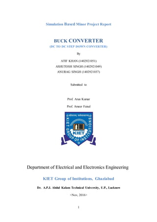
  • 1. 1 Simulation Based Minor Project Report BUCK CONVERTER (DC TO DC STEP DOWN CONVERTER) By ATIF KHAN (1402921051) ASHUTOSH SINGH (1402921049) ANURAG SINGH (1402921037) Submitted to Prof. Arun Kumar Prof. Ameer Faisal Department of Electrical and Electronics Engineering KIET Group of Institutions, Ghaziabad Dr. A.P.J. Abdul Kalam Technical University, U.P., Lucknow <Nov, 2016>
  • 2. 2 CERTIFICATE This is to certify that Simulation Based Minor Project Report entitled โ€œ Simulation of Buck Converter โ€ which is submitted by ATIF KHAN (1402921051), ASHUTOSH SINGH (1402921049), ANURAG SINGH (1402921037), in partial fulfillment of one of the course work of B.Tech 5th Semester (2016-17) in Department of Electrical and Electronics Engineering, KIET Group of Institutions affiliated to Dr. A.P.J. Abdul Kalam Technical University (APJAKTU), Lucknow. Date: 10/11/2016 Supervisor Prof. Arun Kumar Prof. Ameer Faisal
  • 3. 3 ACKNOWLEDGEMENT It gives us a great senseofpleasure to presentthe reportof the B. TechSimulation Based Minor project undertaken during B. Tech. 5th Semester. We owe a special debt of gratitude to our guide Professor Arun Kumar and Prof. Ameer Faisal, Department of Electrical & Electronics Engineering, Krishna Institute of Engineering & Technology, Ghaziabad for his constant support and guidance throughout the courseof our work. His sincerity, thoroughness, and perseverance have been a constant source of inspiration for us. It is only his cognizant efforts that our endeavors have seen the light of the day. We also take the opportunity to acknowledge the contribution of Professor N K Gupta, Head, Department of Electrical & Electronics Engineering, Krishna Institute of Engineering & Technology, Ghaziabad for his full support and assistance to the development of the project. We also do not like to miss the opportunity to acknowledge the contribution of all faculty members of the department for their kind assistance and cooperation during the development of our project. Last but not the least, we acknowledge our friends for their contribution in the completion of the project. Signature Signature Signature Atif Khan Ashutosh Singh Anurag Singh 1402921051 1402921049 1402921037 Date-10/11/16 Date-10/11/16 Date-10/11/16
  • 4. 4 Abstract A Buck Converter is the basic switched-mode power supply topology.The buck converteris a type of DC to Dc Converter that has an output voltage magnitude is less than the input voltage magnitude. The Buck Converter produces voltage ranging from the input voltage to down to Zero voltage. It is widely used throughout the industry to convert higher DC input voltage into lower DC output voltage. Buck Topology: The Buck Converter is the most popular topology used to distribute power in complex systems e.g. computer motherboard, broadband communication board, etc. The output voltage is adjustable based on the Duty cycle of the switching transistor. One possible drawback of this converter is that the switch does not have a terminal at ground; this complicates the driving circuitry. However, this drawback is of no consequenceif the power supply is isolated from the load circuit (if, for example, the supply is a battery) because the supply and diode polarity can simply be reversed. When they can be reversed, the switch can be on either the ground side or the supply side. A buck (step-down) converter: The output voltage is typical of the same polarity of the input and is the lower than the input. Such a non-inverting buck converter use a single inductor for the buck inductor mode. The buck converter has the filter inductor on the output side, which provides a smoothcontinuous output current waveform to the load. This could be considered a qualitative benefit but requires special considerations for big load transients.
  • 5. 5 TABLE OF CONTENTS 1. CERTIFICATE ......................................................................................................................2 2. ACKNOWLEDGEMENT .....................................................................................................3 3. ABSTRACT...........................................................................................................................4 4. INTRODUCTION .................................................................................................................6 5. CIRCUIT DIAGRAM ...........................................................................................................7 6. WORKING ............................................................................................................................7 7. COMPONENT SELECTION................................................................................................9 7.1 INDUCTOR ....................................................................................................................9 7.2 CAPACITOR ...................................................................................................................9 7.3 POWER MOSFET .........................................................................................................11 8. SIMULATION MODELโ€ฆโ€ฆโ€ฆโ€ฆโ€ฆโ€ฆโ€ฆโ€ฆโ€ฆโ€ฆโ€ฆโ€ฆโ€ฆโ€ฆโ€ฆโ€ฆโ€ฆโ€ฆโ€ฆโ€ฆโ€ฆโ€ฆโ€ฆโ€ฆโ€ฆ..12 9. RESULT...............................................................................................................................13 9.1 SIMULATION COMPONENTS SPECIFICATIONS ..................................................14 10. ADVANTAGES ...............................................................................................................15 11. APPLICATIONS..............................................................................................................16 12. REFERENCES ................................................................................................................16
  • 6. 6 Introduction The main applications of this circuit are in regulated dc power supplies, where a negative polarity output may be desired with respectto the common terminals of the input voltage and the average output is lower than the dc input voltage. The output voltage is controlled by controlling the switch duty cycle. The ratio of output voltage to input voltage is given by: Vo /Vin= Dยท(1 /1-D)=Iin/Io โ€ฆ.(1) Where, Vo and Vin are the output and input voltages, respectively. The term Io and Iin are the output and input currents, respectively. The term D is the duty ratio and de๏ฌned as the ratio of the on time of the switch to the total switching period. This shows the output voltage to be higher or lower than the input voltage, based on the duty ratio D. The dc-dc converter inputs an unregulated dc voltage input and outputs a constant or regulated voltage. The regulators can be mainly classified into linear and switching regulators. All regulators have a power transfer stage and a control circuitry to sense the output voltage and adjust the power transfer stage to maintain the constantoutput voltage. Since a feedback loop is necessary to maintain regulation, some type of compensation is required to maintain loop stability.
  • 7. 7 Circuitdiagram The buckconverter is capableof producinga dc outputvoltage which is smaller in magnitude than the dc input voltage. The arrangement for the basic buck converter is as shown in figure 1. Fig.1. Basic Buck Converter WORKING: When the Switch S is on, the input voltage is applied across the inductor and the current in inductor L rises linearly. At this time the capacitor ( C ) supplies the load current, and it is partially discharged. During the second interval when the transistor is off, the voltage across the inductor reverses in polarity and the diode conducts. During this interval, the energy stored in the inductor supplies the load and, additionally, recharges the capacitor. The steady state inductor current and voltage waveform is shown in figure 2.
  • 8. 8 Using the inductor volt balance principle to find the steady state output voltage equation yields VG .TON + VO .TOFF = 0 Vo = T SW = โˆ’ D VG T 1 โˆ’ D OFF The d varies between 0 and 1 and thus output voltage can belower than the input voltage in magnitude. Figure 1. Steady-state inductor voltage and current waveform, buck converter
  • 9. 9 Component Selection 1. Inductor The magnitude of switching ripple in the output voltage in a properly designed DC supply is much less than the dc component. As a result, the output voltage is approximated by its dc componentand the value of inductor can be calculated by using the defining equation of the inductor V = L diL dt Referring back to figure 2 for the steady state inductor current waveform, it can be easily deduced the change in inductor current is its slope times the length of subinterval. โˆ† I = (V - V ) โ‹… D โ‹… T L G O L sw The ripple requirement in inductor current sets the inductor value. Typically โˆ†IL lies in the range of 10-20% of the full load or maximum value of the dc component of IO. The peak inductor current which is equal to the DC component plus the peak to average ripple โˆ† I L/2, flows through the semiconductor switches and is necessary when specifying device ratings. To reduce the peak current a larger value of the inductor is required. A secondary benefit in lowering the ripple current is that it reduces core/inductor, ESR and load losses.
  • 10. 10 2. Capacitor The output section of the buck converter is as shownin figure 3.5.The only steady state component of output capacitor current is that arising from the inductor current ripple. Hence inductor current cannot be neglected when calculating the output voltage ripple. The inductor current contains both a DC and ripple current component. The DC component must flow entirely through the load resistance R. While the AC switching ripple divides between the load resistance R and the filter capacitor C. Figure 2.Output filter section-buck converter The series impedance of R and C at switching frequency is given by Z Rc,C = R C + 1 jฯ‰ C 1 ZRc,C = Rc2 + ฯ‰2 C2 To ensure minimum ripple at rated output load, the equivalent condition states that the series R-C branch impedance appear resistive over the frequency band of
  • 11. 11 switching component. This is the condition ofminimum ripple and is a reason for requiring low ESR Rc2 + 1 << R ฯ‰2 C 2 C >> 1 2 )ฯ‰ (R 2 โˆ’ R C The output voltage ripple requirement puts an upper bound on capacitor ESR. Thus the voltage ripple peak magnitude is estimated by โˆ†V = โˆ† IL โ‹… R c + โˆ† IL 8โ‹… C โ‹… fsw โˆ†V โ‰… โˆ† IL โ‹… R c With the ESR requirement met, the capacitance value can be selected to achieve adequate filtering. Capacitors are typically paralleled to meet the ESR requirement. An alternate approachto reduce โˆ†V is to reduce โˆ†I but this requires a larger value of the inductor. 3. PowerMOSFETselection MOSFETs are used as power switches for their near zero DC gate current and fast switching times. Its turn-on delay time is proportional to Cgs which is illustrated as Ciss minus Crss in datasheets. The delay time is equal to the product of Cgs and impedance of source driving it ignoring any miller effect. It is a requirement to have delay time much less than switching period. MOSFET's power dissipation impacts converter efficiency. This includes Rdsonconduction
  • 12. 12 losses, leakage losses, turn on-off switching and gate transition losses. Rdsonof the power MOSFET determines the current it canhandle without excessive power dissipation. Rdsondirectly affects the converter efficiency. To minimize Rdson, the applied gate signal should be large enough to maintain operation in the linear, triode or ohmic region. MOSFETโ€™s positive temperature coefficients mean conduction loss increases with temperature. A second important consideration when designing gate drive circuitry is due to Cgd, illustrated as Crss in data sheets. During turn-on and turn-off, the large swing in Vgd requires extra current sourcing and sinking capabilities for the gate drive as a direct result of miller effect. Simulation Model:
  • 15. 15 Advantages of Buck & Boost Converter ๏‚ท Gives the high output voltage ๏‚ท Low operating duty cycles ๏‚ท Lower voltage on MOSFET
  • 16. 16 Application ๏‚ท Automotive applications ๏‚ท Power amplifier applications ๏‚ท Adaptive control applications ๏‚ท Battery power systems ๏‚ท Consumer Electronics ๏‚ท Communication Applications References ๏‚ท P.S. Bhimbhra โ€œPower Electronicsโ€-Fifth Edition ๏‚ท M.D. Singh โ€œPower Electronicsโ€-Fourth Edition ๏‚ท Research paper on Buck-Boost Converter