
Recommended
More Related Content
What's hot
What's hot (20)
Similar to Design and Implementation a BPSK Modem and BER Measurement in AWGN Channel
Similar to Design and Implementation a BPSK Modem and BER Measurement in AWGN Channel (20)
More from IJSRP Journal
More from IJSRP Journal (20)
Recently uploaded
Recently uploaded (20)
Design and Implementation a BPSK Modem and BER Measurement in AWGN Channel
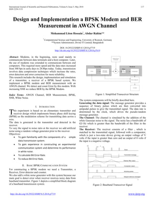
- 1. International Journal of Scientific and Research Publications, Volume 8, Issue 5, May 2018 117 ISSN 2250-3153 http://dx.doi.org/10.29322/IJSRP.8.5.2018.p7719 www.ijsrp.org Design and Implementation a BPSK Modem and BER Measurement in AWGN Channel Mohammad Liton Hossain* , Abdur Rahim** * Computational Science and Engineering, University of Rostock, Germany **System Administrator, Divine IT Limited, Bangladesh DOI: 10.29322/IJSRP.8.5.2018.p7719 http://dx.doi.org/10.29322/IJSRP.8.5.2018.p7619 Abstract- Modems, in the beginning, were used mainly to communicate between data terminals and a host computer. Later, the use of modems was extended to communicate between end computers. This required more speed and the data rates increased from 300 bps in early days to 28.8bps today. Today, transmission involves data compression techniques which increase the rates, error detection and error correction for more reliability. This research includes the design, implementation and simulation of a transmitter, a receiver of a BPSK based system. We implement a BPSK modem and BER measurement with an AWGN channel. We detect and count Error by this modem. With increasing SNR we reduce BER by the BPSK Modem. Index Terms- AWGN Channel, BER Measurement, BPSK, SNR, White Noise. I. INTRODUCTION his experiment is based on an elementary transmitter and receiver design which implements binary phase shift keying (BPSK) as the modulation scheme for transmitting data across a wire. The data is generated in the transmitter and detected in the receiver. To vary the signal to noise ratio at the receiver we add artificial noise using a random voltage generator prior to the receiver. Objectives: • To gain familiarity with the components of a simple data transmission system. • To gain experience in constructing an experimental communication system and determine its performance in white noise. • To calculate Bit Error Rate. • To reduce Bit Error Rate. II. BASIC BPSK COMMUNICATION SYSTEM For constructing a BPSK modem we need a Transmitter, a Receiver, Error detector and counter. We also add a white noise generator with this system because our main goal is detect error when receiver receives noisy data from baseband transmitter. Figure 1 depicts a simplified block diagram of a baseband transmission system. Figure 1: Simplified Transceiver Structure The system components will be briefly described here. Generating the data signal: The message generator provides a sequence of binary pulses which are then converted into antipodal pulses to give the transmitted signal. The data rate is determined by the clock, which drives the pseudo-random message generator. The Channel: The channel is simulated by the addition of the white Gaussian noise to the signal. The noise has a bandwidth of Ѡ Hz which is greater than the bandwidth of the filter in the receiver. The Receiver: The receiver consists of a filter , which is matched to the transmitted signal, followed with a comparator, which is just a two-state device giving an output voltage of V volts if the input is greater than zero and an output of 0 volts if the input is a negative voltage. Figure 2: Baseband Transceiver Signal T
- 2. International Journal of Scientific and Research Publications, Volume 8, Issue 5, May 2018 118 ISSN 2250-3153 http://dx.doi.org/10.29322/IJSRP.8.5.2018.p7719 www.ijsrp.org Under high signal to noise ratio (SNR) values, the comparator will generate the correct data sequence with very small probability of error, although the data transmissions are likely to be displaced slightly from their true positions. To determine the probability of error, the data sequence at the comparator output is compared with the transmitted data sequence. The comparison is made by the error detector, which gives an output pulse for every bit error that occurs. These error pulses are counted over a known time period and the probability of bit error is determined for various SNR values. The SNR values are measured at the input to the detector’s filter. Note from figure 2 that sampling of the detector filter output effectively occurs in the error detector, where an error is defined to occur if the received data has a different polarity to the transmitted data during the period of each sampling pulse. The sampling pulses are aligned in time with the peak signal output from the detector filter and for simplicity are derived directly from the transmitter clock in this laboratory. The operation of the error detector is shown in Figure 3, which shows the waveforms in the presence of severe noise, with errors occurring. Figure 3: Detector with noisy output The BPSK Modem: The Transmitter’s Components: This is where we generate the baseband signal and convert it to a modulated band pass one. Data Sequence Generator: A TTL or CMOS logic shift register could be used as a pseudo-random sequence message generator. In this particular experiment we will utilize the clock pulse to generate a sequence of repetitive ones and zeros, i.e. 10101010……….. First, the clock used in this experiment is devised using an NE555 timer circuit. By choosing resistor values of 1KΩ and 47KΩ and capacitor value of 0.01µF, the circuit produces a square waveform. To generate the message signal of 10101010…………….we feed the clock pulse into a 2n frequency divider circuit implemented using a combination of D-type bistables. The frequency divider circuit is implemented using the SN74LS74 integrated circuit. This particular circuit divides the frequency of the clock signal into four, in other words, it increases the symbol duration by four times the original clock pulse. Sinusoidal Waveform Generator: The sinusoidal signal is required to modulate the square waveform. This usually generated using specially designed oscillators. In this particular experiment we will use a low pass filter circuit to produce a sinusoidal waveform from the correct signal. To achieve this we use an 2nd order Butterworth Lowpass filter. This filter is constructed using the LM741 operational amplifier IC. The transfer function of this filter is given as: Where the cut-off frequency at 3dB is, By choosing a resistor value of 10KΩ and a capacitor value of 4.7nF a cut-off frequency of fc will be obtained. Note that, to obtain a smooth sinusoidal waveform, a second Butterworth filter is needed. Construct and add this second filter in series with the first one. BPSK Modulation Stage: To modulate the phase of the sinusoidal waveform using the message signal ( signal at the output of the frequency divider), we use an analogue switch (DG211 integrated circuit) which has the sinusoidal signal generated in signal generator at one of its inputs and an inverted copy (1800 shifted copy) of this signal at its second input. The message signal is connected to a third input and used to control the analogue switch which produces a 00 shifted sinusoid when the message signal is high and a 1800 shifted sinusoid when the message signal is low. Before connecting the sinusoidal signal to the analogue switch, we remove the DC component of that signal to convert it to a non-return to zero sinusoid. To do this, we pass the signal through a simple RC high pass filter. To generate a 1800 shifted copy of this sinusoid, we pass this signal into an operational amplifier inverter circuit. To produce the BPSK modulated signal, we take both outputs from the analogue switch circuits and connect them to an op-amp adder circuit implemented by the LM741 IC. Note: the analogue switch circuit used contains four switches, some of which used for modulation and some at the receiver. Note: the inverter and adder op-amp circuits are designed to both have a gain of 1 The channel: White Noise Adder The simplest kind of channels available is the memory-less additive white Gaussian noise (AWGN) channels. Additive white Gaussian noise (AWGN) is a channel model in which the only impairment to communication is a linear addition of wideband or white noise with a constant spectral density (expressed as watts per hertz of bandwidth) and a Gaussian distribution of amplitude. The model does not account for fading, frequency selectivity, interference, nonlinearity or dispersion. However, it produces simple and tractable mathematical models which are useful for gaining insight into the underlying behavior of a system before these other phenomena are considered.
- 3. International Journal of Scientific and Research Publications, Volume 8, Issue 5, May 2018 119 ISSN 2250-3153 http://dx.doi.org/10.29322/IJSRP.8.5.2018.p7719 www.ijsrp.org Wideband Gaussian noise comes from many natural sources, such as the thermal vibrations of atoms in conductors (referred to as thermal noise or Johnson-Nyquist noise), shot noise, black body radiation from the earth and other warm objects, and from celestial sources such as the Sun. The AWGN channel is a good model for many satellite and deep space communication links. It is not a good model for most terrestrial links because of multipath, terrain blocking, interference, etc. However, for terrestrial path modeling, AWGN is commonly used to simulate background noise of the channel under study, in addition to multipath, terrain blocking, interference, ground clutter and self-interference that modern radio systems encounter in terrestrial operation. To test our BPSK modem is such channels we use a Gaussian Noise Generator to produce a wideband signal with randomly varying waveform. This noise signal is added onto the BPSK modulated signal using an op-amp adder circuit with a gain of 1. The Receiver’s Components: This is where we detect the modulated band pass signal and demodulated it back to baseband to detect the information transmitted and count the symbol error rate of the system under a variety of different signal to noise power ratio (SNR). RC Low pass filter: The first stage of the receiver then is to pass the BPSK noisy signal through a low pass filter. In this experiment, we use an RC filter with a cut-off frequency equivalent to the transmitted signal’s frequency. The Correlator: The correlator circuit consists of two stages, an analogue multiplier and an op-amp based integrator circuit. The multiplier used as the AD633 IC which has at its inputs both the received signal from the RC low pass filter and the original sinusoidal signal generated or its 1800 inverted image from previous section. The output signal from this multiplier is then passed into the integrator circuit which is re-set to zero at the beginning of every symbol. The resetting of the integrator is performed using the fourth switch in the analogue switch circuit. This switch is left is triggered to close by the pulses delayed to occur at the positive edge and negative edge of every half cycle. The switch remains open during the integration of the remainder of the half cycle. Synchronization (sampling and reset pulses generation): In order to be able to compare both the transmitted signal and the detected one, it is highly important to synchronize both signals using the correct sampling and reset pulses. In this experiment the two types of pulses are generated from the reference data provided by the frequency divider. To generate all the required pulses, three “retriggerable monostable multivibrators” are needed. These can be built using the SN74121 IC circuit. By connecting the monostables as shown in the receiver’s circuit, the error detector’s sampling pulse of width 0.125ms can be obtained from the second monostable. This pulse is generated every half cycle of the reference data which would correspond to the moment when the integrator reaches the most positive (or negative depending on which symbol is being detected) peak voltage. The reset pulse of width 0.08ms (for the analogue switch connected to the integrator circuit of the correlator) can be obtained from the third monostable. This pulse is generated at the beginning of every half cycle to reset the integrator to zero. The Comparator Circuit: The comparator circuit is designed using an op-amp circuit using the LM311 integrated circuit. This circuit produces an output voltage of 5 volts when it receives a positive input and zero volts when it receives a negative input. This results in regenerating the original baseband signal. The Error Detector: This circuit performs a comparison between the signal at the output of the comparator and a delayed copy of the original signal from the frequency divider. It must be noted that this comparison only takes place during the sampling pulse only. If the reference data and the received data have different polarities during the sampling pulse this will produces an error pulse. The error detector is designed using two logic circuits which include an XOR gate DM74LS86 and NAND gate SN7400 ICs. Two monostables, SN7421 ICs, are also used here to generate the delayed version of the reference data. Connecting the monostables as shown in the receiver figure produces an x ms long delayed version of the original data signal at the output of the second monostable. This signal and the received copy from the comparator are connected to the XOR circuit which will only produce a high voltage when the two inputs are different. The output from the XOR is connected to the input of the first NAND gate which also has the sampling pulse connected to its other input. The NAND gate will produce zero voltage at its output only if both inputs are high. The output of this NAND gate is applied to the input of the second NAND gate in the same IC circuit along with a voltage of 5 volts on its second input. If the output of the second NAN gate is high it indicates there is an error otherwise there is no error. This output is connected to the counter to determine the error rate over a certain signal to noise ratio (SNR). • Measure the bit error rate (BER) for different SNR values, where • Compare the measured BER with the theoretically estimated one using: BERtheoretical = 0.5 erfc( ) III. DESIGN AND IMPLEMENTATION Tools and Components: Transmitter: Clock IC NE555, Frequency Divider IC DM74LS74, Op-Amp Inverter IC LM74,
- 4. International Journal of Scientific and Research Publications, Volume 8, Issue 5, May 2018 120 ISSN 2250-3153 http://dx.doi.org/10.29322/IJSRP.8.5.2018.p7719 www.ijsrp.org Analogue Switch IC DG211, Low pass, Butterworth filter IC LM741, Op-Amp Adder IC LM741, Additive white Gaussian noise (AWGN) generator, High pass, filter, Low pass filter, Resistors, Capacitors, Power source, Breadboard, Oscilloscope . Receiver: Low pass filter, Frequency Divider IC 7474, Monostable IC SN74121, Analogue Switch IC DG211, Analogue Multiplier IC AD633, Op-Amp Integrator IC LM311, Error Detector, XOR Gate IC DM74LS86, NAND Gate IC, SN7400, Resistors, Capacitors, Power source, Breadboard, Oscilloscope. Design of Transmitter and Receiver: Transmitter • Arrange all the components needed for the transmitter circuit. • Connect the circuit properly showed in figure 4. • Connect the circuit with a 5V DC power supply. • Use the oscilloscope to observe Transmitter output signal showed in figure 2. Figure 4: the Transmitter’s circuit diagram Receiver • Arrange all of component needed for receiver circuit • Connect the circuit properly showed in figure 5. • Connect the circuit with power supply. • Connect the output of transmitter to the input of the receiver. • Use the oscilloscope to observe the output showed in figure 3. Figure 5: The Receiver’s Circuit Diagram IV. SIMULATION For simulations we have used MATLAB for BPSK Modem BER measurement with AWGN channel and reduce the error rate. BPSK Modulation and Demodulation: Using MATLAB we design BPSK modem modular and demodular. Collect all parameters from MATLAB library and produce a module like following figure Figure 6: the BPSK Modem Modulation and Demodulation The Transmitter output and The Receiver output of BPSK modem shown in figure below Figure 7: Modulated and Demodulated signal curve Bit Error Rate calculation: For BER (Bit Error Rate) calculation we design BPSK modem with AWGN channel. For design this system we need Binary Symmetric Channel block, BPSK Modulator Baseband block, AWGN Channel block, BPSK Demodulator Baseband block, Error Rate Calculation block and a Display block. The combination of system parameters from MATLAB library Shown in figure below:
- 5. International Journal of Scientific and Research Publications, Volume 8, Issue 5, May 2018 121 ISSN 2250-3153 http://dx.doi.org/10.29322/IJSRP.8.5.2018.p7719 www.ijsrp.org Figure 8: the BPSK Modem with AWGN System Parameter 1: Probability of a zero=0.5 Initial seed=61 Sample time=1 Output data type=Double Receive delay=0 Computation delay=0 Target number of errors=100 Maximum number of symbols=1e6 Result: The bit error rate=0.01162 The number of errors=100 The total number of bits that are transmitted=8604 Figure 9: BER measurements with probability 0.5 System Parameter 2 Error probability=0.01 Line seed=2137 SNR 4.2 Result: The bit error rate=0.01184 The number of errors=100 The total number of bits that are transmitted=8447 Figure 10: BER measurement when error probability 0.01 System Parameter 3 Error probability=0.01 Line seed=10 SNR 4.2 Result: The bit error rate=0.01183 The number of errors=100 The total number of bits that are transmitted=8454 Figure 11: BER measurements with changed Line seed System Parameter 4 Error probability=0.01 Line seed=10 SNR=7 Result: The bit error rate=0.0007574 The number of errors=100 The total number of bits that are transmitted=1.32e+005 Figure 12: BER measurements with changed SNR System Parameter 5 Error probability=0.01 Line seed=10 SNR=3 Result: The bit error rate=0.02217 The number of errors=100 The total number of bits that are transmitted=4511 We also measure Bit Error Rate (BER) using MATLAB code. Figure 13 depicts the curve BER Vs Signal to noise ratio (Eb/No). Where the signal to noise ratio denoted by dB form.
- 6. International Journal of Scientific and Research Publications, Volume 8, Issue 5, May 2018 122 ISSN 2250-3153 http://dx.doi.org/10.29322/IJSRP.8.5.2018.p7719 www.ijsrp.org Figure 13: BER Vs EbNo using BPSK in AWGN Channel Reduction of the Error Rate Using Cyclic Code: In coding theory, cyclic codes are linear block error-correcting codes that have convenient algebraic structures for efficient error detection and correction. The Binary Cyclic Encoder block creates a systematic cyclic code with message length K and codeword length N. The number N must have the form 2M-1, where M is an integer greater than or equal to 3. This block accepts a column vector input signal containing K elements. The output signal is a column vector containing N elements. The Binary Cyclic Decoder block recovers a message vector from a codeword vector of a binary systematic cyclic code. For proper decoding, the parameter values in this block should match those in the corresponding Binary Cyclic Encoder block. If the cyclic code has message length K and codeword length N, then N must have the form 2M-1 for some integer M greater than or equal to 3. This block accepts a column vector input signal containing N elements. The output signal is a column vector containing K elements. Here by adding channel coding reduction of error rate has been done in the model shown in the figure 14 BPSK Modulation Model, for certain noise levels. To design this system here we have used Binary Symmetric Channel block, Binary Cyclic Encoder, BPSK Modulator Baseband block, AWGN Channel block, BPSK Demodulator Baseband block, Binary Cyclic Decoder, Error Rate Calculation block and a Display block. Wide window model and connections between the blocks have been shown in the following figure. Figure 14: Reduction of error rate of BPSK modem Calculation Simulation Parameters: Bernoulli Binary Generator: Probability of a zero = 0.01 Samples per frame =21 Binary Cyclic Encoder and decoder: Codeword length N = 31. Message length K = 21. AWGN channel Mode = Signal to Noise Ratio (Eb/No) = 7+10*log10 (21/31) Symbol period = 21/31 Error-Rate Calculation Maximum number of symbols 1e7 Results: The bit error rate=8.025e-005 The number of errors=103 The total number of bits that are transmitted=1.284e+006 Figure 15: Reduction of error rate of BPSK modem in AWGN channel V. CONCLUSION AND FUTURE WORK In this study, the performance of the BPSK modem is to detect error at different data rates. It also counts the BER (Bit Error Rate) at different signal to noise ratios: • It is observed that when Transmitted data is 8604bps then the BER is 0.01162 and total error is 100. In this section Signal to noise ratio is 4.2dB. • It is observed that when Transmitted data is 1.32e+005bps then the BER is 0.0007574. In this section Signal to noise ratio is 7dB. • Finally it is observed that with increasing Signal to Noise Ratio decreasing Bit Error Rate (BER). • In this project, The BPSK modem also reduce error rate using cyclic code. • It is observed that the total number of bits is transmitted is1.284e+006bps then the Bit Error Rate is only 8.025e-005 and the total number of error is 103.
- 7. International Journal of Scientific and Research Publications, Volume 8, Issue 5, May 2018 123 ISSN 2250-3153 http://dx.doi.org/10.29322/IJSRP.8.5.2018.p7719 www.ijsrp.org Following are the areas of future study which can be considered for further research work. • This research can be easily implemented as a Satellite Modem. A satellite modem or sat modem is a modem used to establish data transfers using a communications satellite as a relay. The main functions of a satellite modem are modulation and demodulation. Satellite communication standards also define error correction codes and framing formats. These functions are easily designed by BPSK. • We can use this modem where we need data transmission and detect error. • We can also use this modem to reduce the Bit Error Rate in data communication. ACKNOWLEDGMENT At first all thanks goes to almighty creator who gives me the opportunity, patients and energy to complete this study. I would like to express my sincere gratitude and cordial thanks to the Abdullah-Al-Shamim Assistant professor of IST and Syeda Zinath Aman, lecturer of IST for their constant support, valuable instruction, and helpful advice during the course of studies and research work. Finally, I must express my very profound gratefulness to my parents and to my wife for providing me with constant support and encouragement during my years of study and through the process of researching and writing this paper. This accomplishment would not have been possible without them. Thank you. REFERENCES [1] Louis E. Frenzel, Communication Electronics [2] G. K. Mithal, Radio Engineering (Principle of Communication System) [3] Taub, Schilling saha, Principles of Communication Systems [4] Dr. Rezaul Karim Mazumder, Principles of electronic circuits. [5] Walker H.R. Ultra Narrow Band Modulation Textbook. Available Online: http://www.vmsk.org/ (accessed on 23 July 2008). [6] Wu L.N. Advance in UNB high speed communications. Prog. Nat. Sci. (in Chinese) 2007;17:143–149. [7] Feng M., Wu L.N. Special non-linear filter and extension to Shannon's channel capacity. Digital Signal Proc. 2009;19:861–873. [8] Akiyldiz I., Su W., Sankarasubramaniam Y., Cayirci E. A survey on sensor networks. IEEE Commun. Mag. 2002;40:102–114. [9] Suhinthan M., Saman H, Malin P. Energy efficient sensor scheduling with a mobile sink node for the target tracking application. Sensors. 2009;9:696–716. [10] Alippi C., Anastasi G., Di Francesco M., Roveri M. An adaptive sampling algorithm for effective energy management in wireless sensor networks with energy-hungry sensors. IEEE Instrum. Meas. Mag. 2010;59:335–344. [11] Anastasi G., Conti M., Francesco M., Passarella A. Energy conservation in wireless sensor networks. Ad Hoc Netw. 2009;7:537–568. [12] Wu L.N. UNB modulation in high speed space communications. Proc. SPIE. 2007;6795:679510-1–679510-6. [13] Feng M., Wu L.N., Qi C.H. Analysis and optimization of power spectrum on EBPSK modulation in throughput-efficient wireless system. J. Southeast Univ. 2008;24:143–148. [14] Wu L.N., Feng M., Gao P. An impulse filter method used in ABSK signal. Chinese Patent. 2009 CN10029875.3 [15] Proakis J.G. Digital Communications. 4th ed. McGraw-Hill Book Company, Inc.; Columbus, OH, USA: 2001. [16] Oppenheim A.V., Willsky A.S. Signals and Systems. 2nd ed. Publishing House of Electronics Industry; Beijing, China: 2009. [17] Proakis J.G., Salehi M. Communication System Engineering. 2nd ed. Prentice Hall; Bergen County, NJ, USA: 2002. [18] . Michel Elnaggar, Safieddin Safavi-Naeini, and Sujeet K. Chaudhuri , “Effect of Over Simplifying the Simulated Indoor Propagation on the Deterministic MIMO capacity”, CCECE 2004- CCGEI 2004, Niagara Falls, Mayimai, 2004. [19] www.en.wikipedia.org [20] www.mathworks.com AUTHORS First Author – Mohammad Liton Hossain, M.Sc., Lecturer at Institute of Science and Technology E-Mail: litu702@mail.com Second Author – Abdur Rahim, M.Sc., System Administrator at Divine IT Limited. E-mail: akrahim741@gmail.com