LTE Measurement: How to test a device
•
49 likes•30,453 views

LTE Measurement: How to test a device This course provides an overview with practical examples and exercises on how to test a LTE-capable device while performing standardized RF measurements such as power, signal quality, spectrum and receier sensitivity, and how to automate these measurements in a simple and cost-effective way. We will present testing of LTE handsets in terms of protocol signaling scenarios and handover to other radio technologies for interoperability. This course will demonstrate end-to-end (E2E), throughput and application testing using the Rohde & Schwarz R&S®CMW500 Wideband Radio Communication Tester. Examles of application tests are voice over LTE, (VoLTE) or Video over LTE.

Recommended
Recommended
More Related Content
What's hot
What's hot (20)
Similar to LTE Measurement: How to test a device
Similar to LTE Measurement: How to test a device (20)
More from Rohde & Schwarz North America
More from Rohde & Schwarz North America (20)
Recently uploaded
Recently uploaded (20)
LTE Measurement: How to test a device
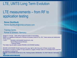
- 1. LTE, UMTS Long Term Evolution LTE measurements – from RF to application testing Reiner Stuhlfauth Reiner.Stuhlfauth@rohde-schwarz.com Training Centre Rohde & Schwarz, Germany Subject to change – Data without tolerance limits is not binding. R&S® is a registered trademark of Rohde & Schwarz GmbH & Co. KG. Trade names are trademarks of the owners. 2011 ROHDE & SCHWARZ GmbH & Co. KG Test & Measurement Division - Training Center - This folder may be taken outside ROHDE & SCHWARZ facilities. ROHDE & SCHWARZ GmbH reserves the copy right to all of any part of these course notes. Permission to produce, publish or copy sections or pages of these notes or to translate them must first be obtained in writing from ROHDE & SCHWARZ GmbH & Co. KG, Training Center, Mühldorfstr. 15, 81671 Munich, Germany
- 2. Mobile Communications: Fields for testing l RF testing for mobile stations and user equipment l RF testing for base stations l Drive test solutions and verification of network planning l Protocol testing, signaling behaviour l Testing of data end to end applications l Audio and video quality testing l Spectrum and EMC testing November 2012 | LTE measurements| 2
- 3. Test Architecture RF-/L3-/IP Application-Test November 2012 | LTE measurements| 3
- 4. LTE: EPS Bearer E-UTRAN EPC Internet UE eNB S-GW P-GW Peer Entity End-to-end Service EPS Bearer External Bearer Radio Bearer S1 Bearer S5/S8 Bearer Radio S1 S5/S8 Gi November 2012 | LTE measurements| 4
- 5. Mobile Radio Testing Adjust the downlink Generate downlink signal to how uplink is Perform signal and send control received RF measurements on commands received uplink Core network A mobile radio tester emulates a base station November 2012 | LTE measurements| 5
- 6. Mobile Radio Testing Generate downlink Generate downlink signal and send signal signaling information No signaling Control PC Signaling testing Non-Signaling testing November 2012 | LTE measurements| 6
- 7. LTE measurements general aspects November 2012 | LTE measurements| 7
- 8. LTE RF Testing Aspects UE requirements according to 3GPP TS 36.521 Power Transmit signal quality Maximum output power Frequency error Maximum power reduction Modulation quality, EVM Additional Maximum Power Carrier Leakage Reduction In-Band Emission for non allocated RB Minimum output power EVM equalizer spectrum flatness Configured Output Power Output RF spectrum emissions Power Control Occupied bandwidth Absolution Power Control Out of band emissions Relative Power Control Aggregate Power Control Spectrum emisssion mask ON/OFF Power time mask Additional Spectrum emission mask Adjacent Channel Leakage Ratio 36.521: User Equipment (UE) radio transmission and reception Transmit Intermodulation November 2012 | LTE measurements| 8
- 9. LTE RF Testing Aspects UE requirements according to 3GPP, cont. Receiver characteristics: Reference sensitivity level Maximum input level Adjacent channel selectivity Blocking characteristics In-band Blocking Out of band Blocking Narrow Band Blocking Spurious response Intermodulation characteristics Spurious emissions Performance November 2012 | LTE measurements| 9
- 10. LTE RF Testing Aspects BS requirements according to 3GPP l Transmitter Characteristics l Base station output power l Frequency error l Output power dynamics l Transmit ON/OFF power l Output RF spectrum emissions (Occupied bandwidth, Out of band emission, BS Spectrum emission mask, ACLR, Spurious emission, Co-existence scenarios,…) l Transmit intermodulation l Modulation quality TR 36.804: Base Station (BS) radio transmission and reception November 2012 | LTE measurements| 10
- 11. LTE RF Testing Aspects BS requirements according to 3GPP, cont. l Receiver Characteristics l Reference sensitivity level l Dynamic range l Adjacent Channel Selectivity (ACS) l Blocking characteristics l Intermodulation characteristics l Spurious emissions l Performance November 2012 | LTE measurements| 11
- 12. LTE RF Measurements – regional requirements l Regional / band-specific requirements exist (e.g. spurious emissions) l Since UEs roam implementation has to be dynamic Concept of network signaled RF requirements has been introduced with LTE. - Network signaled value: NS_01 … NS_32 - transmitted as IE AdditionalSpectrumEmission in SIB2 November 2012 | LTE measurements| 12
- 13. LTE bands and channel bandwidth E-UTRA band / channel bandwidth E-UTRA Band 1.4 MHz 3 MHz 5 MHz 10 MHz 15 MHz 20 MHz 1 Yes Yes Yes Yes 2 Yes Yes Yes Yes Yes[1] Yes[1] 3 Yes Yes Yes Yes Yes[1] Yes[1] 4 Yes Yes Yes Yes Yes Yes 5 Yes Yes Yes Yes[1] 6 Yes Yes[1] 7 Yes Yes Yes Yes[1] 8 Yes Yes Yes Yes[1] 9 Yes Yes Yes[1] Yes[1] 10 Yes Yes Yes Yes 11 Yes Yes[1] 12 Yes Yes Yes[1] Yes[1] 13 14 Yes[1] Yes[1] Yes[1] Yes[1] Not every channel ... 17 Yes[1] Yes[1] bandwidth for ... every band! 33 Yes Yes Yes Yes 34 Yes Yes Yes 35 Yes Yes Yes Yes Yes Yes 36 Yes Yes Yes Yes Yes Yes 37 Yes Yes Yes Yes 38 Yes Yes Yes Yes 39 Yes Yes Yes Yes 40 Yes Yes Yes Yes NOTE 1: bandwidth for which a relaxation of the specified UE receiver sensitivity requirement (Clause 7.3) is allowed. November 2012 | LTE measurements| 13
- 14. Tests performed at “low, mid and highest frequency” Nominal frequency RF power described by EARFCN (E-UTRA Absolute lowest EARFCN possible Radio Frequency Channel Number) and 1 RB at position 0 Frequency = whole LTE band RF power mid EARFCN and 1 RB at position 0 Frequency RF power Highest EARFCN and 1 RB at max position Frequency November 2012 | LTE measurements| 14
- 15. Test Environment – Test System Uncertainty 36.101 / 36.508 • Temperature/Humidity -normal conditions +15C to +35C, relative humidity 25 % to 75 % -extreme conditions -10C to +55C (IEC 68-2-1/68-2-2) • Voltage • Vibration Acceptable Test System Uncertainty (Test Tolerance, TT) defined for each test individually in 36.521 Annex F (will be ignored further on for the sake of simplicity) Test Minimum Requirement in TS Test Test Requirement in TS 36.521- 36.101 Tolerance 1 (TT) 6.2.2. UE Power class 1: [FFS] 0.7 dB Formula: Maximum Output Power class 2: [FFS] 0.7 dB Upper limit + TT, Lower limit - TT Power Power class 3: 23dBm ±2 dB 0.7 dB Power class 1: [FFS] Power class 4: [FFS] 0.7 dB Power class 2: [FFS] Power class 3: 23dBm ±2.7 dB Power class 4: [FFS] November 2012 | LTE measurements| 15
- 16. LTE RF measurements on base stations November 2012 | LTE measurements| 16
- 17. OFDM risk: Degradation Channel (ideal) sl n rl n 1 TMC Samples f f0 f1 f2 f3 f0 f1 f2 f3 November 2012 | LTE measurements| 17
- 18. OFDM risk: Degradation due to Frequency Offset Channel e j 2fn sl n rl n f Samples f f0 f1 f2 f3 f0 f1 f2 f3 November 2012 | LTE measurements| 18
- 19. OFDM risk: Degradation due to Clock Offset Channel sl n rl n f k Samples f f0 f1 f2 f3 f0 f1 f2 f3 November 2012 | LTE measurements| 19
- 20. Subcarrier zero handling Subcarrier 0 or DC subcarrier causes problems in DAC for direct receiver strategies, DC offset! Downlink: f-1 f+1 1 j 2kf t N CP ,l Ts N RB Nsc / 2 DL RB sl( p ) t ak (p)) ,l e ( ak( (p)) ,l e j 2kf t NCP ,lTs DC subcarrier, k N RB N sc / 2 DL RB k 1 suppressed 1/TSYMBOL=15kHz Uplink: N RB Nsc / 2 1 UL RB j 2 k 1 2 f t N CP ,l Ts sl t a k ( ) ,l e k N RB N sc / 2 UL RB f-1 f0 f1 f ½ subcarrier DC subcarrier offset November 2012 | LTE measurements| 20
- 21. LTE: DC subcarrier usage DC subcarrier or subcarrier 0 is not used in downlink! November 2012 | LTE measurements| 21
- 22. DC offset – possible reasons DC offset originated by mixer: fBB=fRx-fLO fRX=fLO+fBB+fLO_ɛ 1st mixer fLO –fLO_ɛ=DC fBB + DC Non-linearities of fLO_ɛ fLO Amplifier also cause DC in the signal PLL Idea: set PLL to frequency fLO to get frequency of baseband as fBB = fRX – fLO But: if synthesizer has leakage: fLO_ɛ will spread into the input: At the output we get direct current, DC! November 2012 | LTE measurements| 22
- 23. Base station test models Parameter 1.4 MHz 3 MHz 5 MHz 10 MHz 15 MHz 20 MHz Reference, Synchronisation Signals RS boosting, PB = EB/EA 1 1 1 1 1 1 Synchronisation signal EPRE / ERS [dB] 0.000 0.000 0.000 0.000 0.000 0.000 Reserved EPRE / ERS [dB] -inf -inf -inf -inf -inf -inf PBCH PBCH EPRE / ERS [dB] 0.000 0.000 0.000 0.000 0.000 0.000 Reserved EPRE / ERS [dB] -inf -inf -inf -inf -inf -inf PCFICH # of symbols used for control channels 2 1 1 1 1 1 PCFICH EPRE / ERS [dB] 3.222 0 0 0 0 0 PHICH # of PHICH groups 1 1 1 2 2 3 # of PHICH per group 2 2 2 2 2 2 PHICH BPSK symbol power / ERS [dB] -3.010 -3.010 -3.010 -3.010 -3.010 -3.010 PHICH group EPRE / ERS [dB] 0 0 0 0 0 0 PDCCH # of available REGs 23 23 43 90 140 187 # of PDCCH 2 2 2 5 7 10 # of CCEs per PDCCH 1 1 2 2 2 2 TS 36.141 # of REGs per CCE 9 9 9 9 9 9 # of REGs allocated to PDCCH 18 18 36 90 126 180 Defines several # of <NIL> REGs added for padding 5 5 7 0 14 7 Test models PDCCH REG EPRE / ERS [dB] 0.792 2.290 1.880 1.065 1.488 1.195 <NIL> REG EPRE / ERS [dB] -inf -inf -inf -inf -inf -inf For base station PDSCH # of QPSK PDSCH PRBs which are boosted 6 15 25 50 75 100 e.g. E-TM1.1 PRB PA = EA/ERS [dB] 0 0 0 0 0 0 # of QPSK PDSCH PRBs which are de-boosted 0 0 0 0 0 0 PRB PA = EA/ERS [dB] n.a. n.a. n.a. n.a. n.a. n.a. November 2012 | LTE measurements| 23
- 24. Base station unwanted emissions Spurious emissions ACLR •Adjacent channel leakage •Operating band unwanted emissions Channel Spurious domain ΔfOOB bandwidth ΔfOOB Spurious domain RB E-UTRA Band Worst case: Ressource Blocks allocated at channel edge November 2012 | LTE measurements| 24
- 25. Adjacent Channel Leakage Ratio - eNB E-UTRA transmitted BS adjacent channel Assumed Filter on the ACLR signal channel centre adjacent adjacent lim bandwidth frequency offset channel channel it BWChannel [MHz] below the first carrier frequency and or above the last (informative) corresponding carrier centre filter bandwidth frequency transmitted 1.4, 3.0, 5, 10, 15, 20 BWChannel E-UTRA of same Square (BWConfig) 45 dB BW 2 x BWChannel E-UTRA of same Square (BWConfig) 45 dB BW BWChannel /2 + 2.5 3.84 Mcps UTRA RRC (3.84 Mcps) 45 dB MHz BWChannel /2 + 7.5 3.84 Mcps UTRA RRC (3.84 Mcps) 45 dB MHz NOTE 1: BWChannel and BWConfig are the channel bandwidth and transmission bandwidth configuration of the E-UTRA transmitted signal on the assigned channel frequency. Large bandwidth NOTE 2: The RRC filter shall be equivalent to the transmit pulse shape filter defined in TS 25.104 [6], with a chip rate as defined in this table. Limit is either -13 / -15dBm absolute or as above November 2012 | LTE measurements| 25
- 26. Adjacent channel leakage power ratio November 2012 | LTE measurements| 26
- 27. ACLR measurement * RBW 10 kHz VBW 30 kHz Ref 0 dBm Att 25 dB SWT 250 ms 0 * A -10 1 AP VIEW -20 2 AP VIEW -30 3 AP CLRWR -40 -50 EXT UTRAACLR1 UTRAACLR2 = 33 dB = 36 dB UTRAACLR2bis 3DB = 43 dB -60 -70 -80 -90 Additional requirement for E-UTRA frequency band I, -100 signaled by network to the UE Center 1.947 GHz 2.5 MHz/ Span 25 MHz fUTRA, ACLR2 fUTRA, ACLR1 fCarrier November 2012 | LTE measurements| 27 Date: 21.AUG.2008 15:51:00
- 28. Operating band unwanted emissions Narrow bandwidth Frequency offset Frequency offset of Minimum requirement Measurem of measurement measurement filter centre ent filter -3dB point, f frequency, f_offset bandwidth (Note 1) 0 MHz f < 5 0.05 MHz f_offset < 5.05 100 kHz 7 f _ offset MHz MHz 7dBm 0.05 dB 5 MHz 5 MHz f < 5.05 MHz f_offset < -14 dBm 100 kHz min(10 MHz, min(10.05 MHz, fmax) f_offsetmax) 10 MHz f 10.05 MHz f_offset < -16 dBm (Note 5) 100 kHz fmax f_offsetmax TS 36.104 defines several limits: depending on Channel bandwidth, additional regional limits and node B limits category A or B for ITU defined regions => Several test setups are possible! November 2012 | LTE measurements| 28
- 29. Operating band unwanted emissions November 2012 | LTE measurements| 29
- 30. Unwanted emissions – spurious emission The transmitter spurious emission limits apply from 9 kHz to 12.75 GHz, excluding the frequency range from 10 MHz below the lowest frequency of the downlink operating band up to 10 MHz above the highest frequency of the downlink operating band Frequency range Maximum level Measurement Note Bandwidth 9kHz - 150kHz 1 kHz Note 1 150kHz - 30MHz 10 kHz Note 1 -13 dBm 30MHz - 1GHz 100 kHz Note 1 1GHz – 12.75 GHz 1 MHz Note 2 NOTE 1: Bandwidth as in ITU-R SM.329 [5] , s4.1 NOTE 2: Bandwidth as in ITU-R SM.329 [5] , s4.1. Upper frequency as in ITU-R SM.329 [5] , s2.5 table 1 Spurious emission limits, Category A November 2012 | LTE measurements| 30
- 31. Spurious emissions – operating band excluded November 2012 | LTE measurements| 31
- 32. Base station maximum power In normal conditions, the base station maximum output power shall remain within +2 dB and -2 dB of the rated output power declared by the manufacturer. Towards External External antenna connector PA device BS e.g. cabinet TX filter (if any) (if any) Test port A Test port B Normal port for Port to be used for measurements measurements in case external equipment is used November 2012 | LTE measurements| 32
- 33. LTE – DVB interference scenarios Adjacent channel leakage of Basestation x into DTT channel N is point of interest For a BS declared to support Band 20 and to operate in geographic areas within the CEPT in which frequencies are allocated to broadcasting (DTT) service, the manufacturer shall additionally declare the following quantities associated with the applicable test conditions of Table 6.6.3.5.3-4 and information in annex G of [TS 36.104] : PEM,N Declared emission level for channel N P10MHz Maximum output Power in 10 MHz November 2012 | LTE measurements| 33
- 34. Base station receiver test Example: Rx test, moving condition 70% of required throughput of FRC, Fixed Reference Channel November 2012 | LTE measurements| 34
- 35. Base station receiver test – HARQ multiplexing UE sends PUSCH with alternating data and data with multiplexed ACK November 2012 | LTE measurements| 35
- 36. Base station test – power dynamics Synchronisation time/frequency BS under Test FFT 2048 Per Symbol 100 subcarrier Detection / RF- CP- RBs, Ampl. decoding correc- remov 1200 /Phase tion sub correction carr EVM Resource element Tx RETP power: Distinguish: •OFDM symbol •Reference symbol November 2012 | LTE measurements| 36
- 37. Downlink Power Reference Signal: Cell-specific PDCCH power PDSCH power to RS, where NO reference referenceSignalPower depending signals are present, is UE specific and (-60…+50dBm), on ρB/ρA signaled by higher layers as PA. signaled in SIB Type 2 For PDSCH power in same [Power] symbol as reference signal an additional cell specific offset is applied, that is signaled by -50.00 dBm higher layers as PB. PA = -4.77 dB 2011 © Rohde&Schwarz -54.77 dBm PB = 3 (-3.98 dB) -58.75 dBm 0 1 2 3 4 5 6 7 8 9 10 11 12 13 [Time] OFDM symbols RS EPRE = Reference Signal Reference signal power = linear average of all Ref. Energy per Resource Element Symbols over whole channel bandwidth EPRE PDSCH A / B EPRE RS B PB A A PA (with some exeptions for MIMO) November 2012 | LTE measurements| 37
- 38. Base station test – output power dynamics Measure avg OFDM symbol power + Compare active and non-active case Ref. Symbol, always on OFDM Symbol not active! OFDM Symbol active! PDSCH # of 64QAM PDSCH PRBs within a slot for which EVM is measured 1 1 1 1 1 1 Test model: PRB PA = EA/ERS [dB] 0 0 0 0 0 0 E-TM3.1 # of PDSCH PRBs which are not allocated 5 14 24 49 74 99 All RB allocated Test model: PDSCH # of 64QAM PDSCH PRBs within a slot for which EVM 6 15 25 50 75 100 E-TM2 is measured Only 1 RB allocated November 2012 | LTE measurements| 38
- 39. DL Modulation quality: Constellation diagram LTE downlink: several channels can be seen (example): PDSCH with 16 QAM PDCCH + PBCH with QPSK S-SCH with BPSK CAZAC Sequences, Reference signals November 2012 | LTE measurements| 39
- 40. LTE RF measurements on user equipment UEs November 2012 | LTE measurements| 40
- 41. LTE Transmitter Measurements 1 Transmit power 1.1 UE Maximum Output Power 1.2 Maximum Power Reduction (MPR) 1.3 Additional Maximum Power Reduction (A-MPR) 1.4 Configured UE transmitted Output Power 2 Output Power Dynamics 2.1 Minimum Output Power 2.2 Transmit OFF power 2.3 ON/OFF time mask 2.3.1 General ON/OFF time mask 2.3.2 PRACH time mask 2.3.3 SRS time mask 2.4 Power Control 2.4.1 Power Control Absolute power tolerance 2.4.2 Power Control Relative power tolerance 2.4.3 Aggregate power control tolerance 3 Transmit signal quality 3.1 Frequency Error 3.2 Transmit modulation 3.2.1 Error Vector Magnitude (EVM) 3.2.2 Carrier leakage 3.2.3 In-band emissions for non allocated RB 3.2.4 EVM equalizer spectrum flatness 4 Output RF spectrum emissions 4.1 Occupied bandwidth 4.2 Out of band emission 4.2.1 Spectrum Emission Mask 4.2.2 Additional Spectrum Emission Mask 4.2.3 Adjacent Channel Leakage power Ratio 4.3 Spurious emissions 4.3.1 Transmitter Spurious emissions 4.3.2 Spurious emission band UE co-existence 4.3.3 Additional spurious emissions 5 Transmit intermodulation November 2012 | LTE measurements| 41
- 42. UE Signal quality – symbolic structure of mobile radio tester MRT Test equipment Rx TxRx EVM … … … equalizer IDFT meas. DUT RF correction FFT Inband- … … … emmissions l Carrier Frequency error l EVM (Error Vector Magnitude) l Origin offset + IQ offset l Unwanted emissions, falling into non allocated resource blocks. l Inband transmission l Spectrum flatness November 2012 | LTE measurements| 42
- 43. UL Power Control: Overview UL-Power Control is a combination of: l Open-loop: UE estimates the DL-Path- loss and compensates it for the UL l Closed-loop: in addition, the eNB controls directly the UL- Power through power- control commands transmitted on the DL November 2012 | LTE measurements| 43
- 44. PUSCH power control l Power level [dBm] of PUSCH is calculated every subframe i based on the following formula out of TS 36.213 MPR Maximum allowed UE power in this particular cell, Combination of cell- and UE-specific PUSCH transport but at maximum +23 dBm1) components configured by L3 format Number of allocated Cell-specific Downlink Power control resource blocks (RB) parameter path loss adjustment derived Transmit power for PUSCH configured by L3 estimate from TPC command in subframe i in dBm received in subframe (i-4) Bandwidth factor Basic open-loop starting point Dynamic offset (closed loop) 1) +23 dBm is maximum allowed power in LTE according to TS 36.101, corresponding to power class 3bis in WCDMA November 2012 | LTE measurements| 44
- 45. Pcmax definition „upper“ tolerance „lower“ tolerance „corrected“ UE power PCMAX_L– T(PCMAX_L) ≤ PCMAX ≤ PCMAX_H + T(PCMAX_H) PCMAX_L = min{PEMAX_L, PUMAX } PCMAX_H = min{PEMAX_H, PPowerClass} Max. power permitted Max. power in cell, permitted in cell considering bandwidth confinement Max. power for UE Max. power for UE, considering maximum power reduction November 2012 | LTE measurements| 45
- 46. Pcmax definition PCMAX_L– T(PCMAX_L) ≤ PCMAX ≤ PCMAX_H + T(PCMAX_H), lPCMAX_L = min{PEMAX_L , PUMAX }, l PEMAX_L is the maximum allowed power for this particular radio cell configured by higher layers and corresponds to P-MAX information element (IE) provided in SIB Type1 l l PEMAX_L is reduced by 1.5 dB when the transmission BW is confined within FUL_low and FUL_low+4 MHz or FUL_high – 4 MHz and FUL_high, PPowerClass + 2dB 23dBm PPowerClass - 2dB -1.5dB -1.5dB FUL_low FUL_high- 4MHz FUL_high November 2012 | LTE measurements| 46
- 47. Pcmax definition PCMAX_L– T(PCMAX_L) ≤ PCMAX ≤ PCMAX_H + T(PCMAX_H), PCMAX_L = min{PEMAX_L , PUMAX }, l PUMAX corresponds to maximum power (depending on power class, taking into account Maximum Power Reduction MPR and additional A-MPR UE may decide to reduce power UE power class Network may signal = 23dBm ±2 dB bandwidth restriction NS_0x November 2012 | LTE measurements| 47
- 48. UE Maximum Power Reduction UE transmits at maximum power, maximum allowed TX power reduction is given as Modulation Channel bandwidth / Transmission bandwidth configuration MPR (dB) [RB] 1.4 3.0 5 10 15 20 MHz MHz MHz MHz MHz MHz QPSK >5 >4 >8 > 12 > 16 > 18 ≤1 16 QAM ≤5 ≤4 ≤8 ≤ 12 ≤ 16 ≤ 18 ≤1 16 QAM Full >5 >4 >8 > 12 > 16 > 18 ≤2 Higher order modulation schemes require more dynamic -> UE will slightly repeal its confinement for maximum power November 2012 | LTE measurements| 48
- 49. UE Additional Maximum Power Reduction A-MPR Additional maximum Network Requirements E-UTRA Band Channel Resource A-MPR (dB) Signaling (sub-clause) Bandwidth Blocks power reduction value (MHz) requirements can be NS_01 NA NA NA NA NA signaled by the 6.6.2.2.3.1 2,4,35,36 3 >5 ≤1 network as NS value 6.6.2.2.3.1 2,4,10,35,36 5 >6 ≤1 in SIB2 NS_03 6.6.2.2.3.1 2,4,10,35,36 10 >6 ≤1 (IE AdditionalSpectrumEmission) 6.6.2.2.3.1 2,4,10,35,36 15 >8 ≤1 6.6.2.2.3.1 2,4,10,35,36 20 >10 ≤1 NS_04 6.6.2.2.3.2 TBD TBD TBD TBD NS_05 6.6.3.3.3.1 1 10,15,20 ≥ 50 for QPSK ≤1 NS_06 6.6.2.2.3.3 12, 13, 14, 17 1.4, 3, 5, 10 n/a n/a 6.6.2.2.3.3 Table NS_07 13 10 Table 6.2.4.3-2 6.6.3.3.3.2 6.2.4.3-2 > 29 ≤1 NS_08 6.6.3.3.3.3 19 10, 15 > 39 ≤2 > 44 ≤3 [NS_09] 6.6.3.3.3.4 21 TBD TBD TBD .. NS_32 - - - - - November 2012 | LTE measurements| 49
- 50. PUSCH power control Transmit output power ( PUMAX), cont’d. 3GPP Band 13 746 756 777 787 DL UL Network Requiremen Channel E-UTRA Resources A-MPR Signalling ts bandwidth Band Blocks (dB) Value (sub-clause) (MHz) … … … … … … Table Table 6.6.2.2.3 NS_07 13 10 6.2.4 6.2.4 6.6.3.3.2 -2 -2 Indicates the lowest RB … … … … … … index of transmitted Region A Region B Region C resource blocks RBStart 0 – 12 13 – 18 19 – 42 43 – 49 Defines the length of a contiguous RB allocation LCRB [RBs] 6–8 1 – 5 to 9 – 50 ≥8 ≥18 ≤2 A-MPR [dB] 8 12 12 6 3 l In case of EUTRA Band 13 depending on RB allocation as well as number of contiguously allocated RB different A-MPR needs to be considered. November 2012 | LTE measurements| 50
- 51. Pcmax definition – tolerance values PCMAX_L– T(PCMAX_L) ≤ PCMAX ≤ PCMAX_H + T(PCMAX_H) PCMAx Tolerance (dBm) T(PCMAX) (dB) 21 ≤ PCMAX ≤ 23 2.0 Tolerance is 20 ≤ PCMAX < 21 2.5 depending on 19 ≤ PCMAX < 20 3.5 power levels 18 ≤ PCMAX < 19 4.0 13 ≤ PCMAX < 18 5.0 8 ≤ PCMAX < 13 6.0 -40 ≤ PCMAX < 8 7.0 November 2012 | LTE measurements| 51
- 52. Pcmax definition – tolerance values PCMAX_L– T(PCMAX_L) ≤ PCMAX ≤ PCMAX_H + T(PCMAX_H) PCMAX_H = min{PEMAX_H , PPowerClass }, l PEMAX_H is the maximum allowed power for this particular radio cell configured by higher layers and corresponds to P-MAX information element (IE) provided in SIB Type 1 UE power class = 23dBm ±2 dB November 2012 | LTE measurements| 52
- 53. Pcmax definition – tolerance values PCMAX_L– T(PCMAX_L) ≤ PCMAX ≤ PCMAX_H + T(PCMAX_H) PCMAX_H = min{PEMAX_H , PPowerClass }, l PPowerClass. There is just one power class specified for LTE, corresponding to power class 3bis in WCDMA with +23 dBm ± 2dB, MPR and A-MPR are not taken into account, Class 1 Tolerance Class 2 Tolerance Class 3 Tolerance (dB) Class 4 Tolerance (dB) EUTRA (dB (dB) (dBm) (dB) (dBm (dBm) band m) ) 1 23 ±2 2 23 ±22 … 23 ±22 40 23 ±2 November 2012 | LTE measurements| 53
- 54. Pcmax value for power control - analogies PCMAX_L– T(PCMAX_L) ≤ PCMAX ≤ PCMAX_H + T(PCMAX_H) PCMAX_L = min{PEMAX_L, PUMAX } PCMAX_H = min{PEMAX_H, PPowerClass} Maximum speed = 280 km/h =PPowerClass Under those conditions, I shall drive more carefully! Not going to the max seed! =PEMAX_H =PEMAX_L =PUMAX -> speed reduction November 2012 | LTE measurements| 54
- 55. LTE RF Testing: UE Maximum Power UE transmits with 23dBm ±2 dB QPSK modulation is used. All channel bandwidths are tested separately. Max power is for all band classes Test is performed for varios uplink allocations November 2012 | LTE measurements| 55
- 56. Resource Blocks number and maximum RF power 1 active resource block (RB), Nominal RF power band width One active resource block 10 MHz = 50 RB’s (RB) provides maximum absolute RF power Frequency More RB’s in use will be at RF power lower RF power in order to create same integrated power Frequency RF power Additionally, MPR (Max. Power Reduction) and A- MPR MPR are defined Frequency November 2012 | LTE measurements| 56
- 57. UE Maximum Output Power – Test Configuration Initial Conditions Test Environment as specified in TS 36.508 subclause 4.1 Normal, TL/VL, TL/VH, TH/VL, TH/VH Temperature/Voltage Test Frequencies as specified in TS 36.508 subclause 4.3.1 Low range, Mid range, High range high/low Test Channel Bandwidths as specified in TS 36.508 subclause 4.3.1 Lowest, 5MHz, Highest Test Parameters for Channel Bandwidths Downlink Configuration Uplink Configuration Ch BW N/A for Max UE output power testing Mod’n RB allocation FDD TDD 1.4MHz QPSK 1 1 1.4MHz QPSK 5 5 3MHz QPSK 1 1 3MHz QPSK 4 4 5MHz QPSK 1 1 5MHz QPSK 8 8 10MHz QPSK 1 1 10MHz QPSK 12 12 15MHz QPSK 1 1 15MHz QPSK 16 16 20MHz QPSK 1 1 20MHz QPSK 18 18 November 2012 | LTE measurements| 57
- 58. UE maximum power PPowerClass + 2dB 23dBm PPowerClass - 2dB maximum output FUL_high FUL_low power for any transmission bandwidth within the channel bandwidth November 2012 | LTE measurements| 58
- 59. UE maximum power – careful at band edge! PPowerClass + 2dB 23dBm PPowerClass - 2dB -1.5dB -1.5dB FUL_low FUL_high- 4MHz FUL_high FUL_low+4MHz For transmission bandwidths confined within FUL_low and FUL_low + 4 MHz or FUL_high – 4 MHz and FUL_high, the maximum output power requirement is relaxed by reducing the lower tolerance limit by 1.5 dB November 2012 | LTE measurements| 59
- 60. UE maximum power - examples Example 1: No maximum power reduction by higher layers PCMAX_L– T(PCMAX_L) ≤ PCMAX ≤ PCMAX_H + T(PCMAX_H) PCMAX_L = min{PEMAX_L, PUMAX } PCMAX_H = min{PEMAX_H, PPowerClass} Max. power permitted in cell, Max. power for UE, Max. power permitted in Max. power for UE considering bandwidth considering maximum power cell confinement reduction PEMAX_L = none PUMAX = power class 3 = +23 dBm T(PCMAX_L) = T(PCMAX_H)=2dB PEMAX_H = none PPowerClass = power class 3 = +23 dBm PPowerClass + 2dB 25dBm 23dBm PPowerClass - 2dB 21dBm FUL_low FUL_high November 2012 | LTE measurements| 60
- 61. UE maximum power - examples Example 2: max cell power = 0 dBm + band edge maximum power reduction PCMAX_L– T(PCMAX_L) ≤ PCMAX ≤ PCMAX_H + T(PCMAX_H) PCMAX_L = min{PEMAX_L, PUMAX } PCMAX_H = min{PEMAX_H, PPowerClass} PEMAX_L = 0dBm -1.5 dB relaxation = -1.5dBm PEMAX_H = 0 dBm PUMAX = power class 3 – band relaxation = +21.5 dBm PPowerClass = power class 3 = +23 dBm PCMAX_L=-1.5dBm PCMAX_H=0 dBm T(PCMAX_L) = T(PCMAX_H)=7dB PCMAX_H + 7dB +7dBm 0 dBm PCMAX_L - 7dB -8.5dBm FUL_low FUL_low+4MHz FUL_high November 2012 | LTE measurements| 61
- 62. UE maximum power - examples Example 3: Band 13 with NS_07 signalled ( = A-MPR). No Max Power restriction 16 QAM, 12 Resource blocks and RB start = 13. Bandwidth = 10 MHz MPR = 1dB, A-MPR = 12 dB, no band edge relaxation PCMAX_L– T(PCMAX_L) ≤ PCMAX ≤ PCMAX_H + T(PCMAX_H) PCMAX_H = min{PEMAX_H, PPowerClass} PCMAX_L = min{PEMAX_L, PUMAX } PEMAX_L = none PEMAX_H = none PUMAX = power class 3 – MPR – A.MPR = +10 dBm PPowerClass = power class 3 = +23 dBm PCMAX_L=10 dBm T(PCMAX_L) = 6 dB PCMAX_H=23 dBm +25dBm T(PCMAX_H)=2dB PCMAX_H +2dB 23 dBm PCMAX_L - 6dB 4 dBm RB start = 13 12 Resource blocks FUL_high November 2012 | LTE measurements| 62
- 63. UE maximum power - examples Example 4: band edge power relaxation – no higher layer reduction signalled QPSK, 15 RBs allocated, Band 2, RB allocated at band edge MPR = 1dB, A-MPR = 1 dB, band edge relaxation of 1.5dB PCMAX_L– T(PCMAX_L) ≤ PCMAX ≤ PCMAX_H + T(PCMAX_H) PCMAX_L = min{PEMAX_L, PUMAX } PCMAX_H = min{PEMAX_H, PPowerClass} PEMAX_L =none PEMAX_H = none PUMAX = power class 3 – MPR-A-MPR-band relaxation PPowerClass = power class 3 = +23 dBm = 23-1-1-1.5=+19.5 dBm PCMAX_H= 23 dBm PCMAX_L=19.5dBm PCMAX_H + 2dB +25 dBm T(PCMAX_L) = 3.5 dB T(PCMAX_H)=2dB 23 dBm PCMAX_L – 2 dB PCMAX_L – 3.5 dB +16 dBm FUL_low FUL_low+4MHz FUL_high November 2012 | LTE measurements| 63
- 64. LTE RF Testing: UE Minimum Power UE transmits with -40dBm All channel bandwidths are tested separately. Minimum power is for all band classes < -39 dBm November 2012 | LTE measurements| 64
- 65. LTE RF Testing: UE Off Power The transmit OFF power is defined as the mean power in a duration of at least one sub-frame (1ms) excluding any transient periods. The transmit OFF power shall not exceed the values specified in table below Channel bandwidth / Minimum output power / measurement bandwidth 1.4 3.0 5 10 15 20 MHz MHz MHz MHz MHz MHz Transmit OFF power -50 dBm Measurement 1.08 MHz 2.7 MHz 4.5 MHz 9.0 MHz 13.5 MHz 18 MHz bandwidth November 2012 | LTE measurements| 65
- 66. Power Control Related test items l Absolute Power Control Tolerance -- PUSCH open loop power control l Relative Power Control Tolerance – PUSCH relative power control, including both power ramping and power change due to Ressource block allocation change or TPC commands l Aggregate Power Control – PUSCH and PUCCH power control ability when RB changes every subframe November 2012 | LTE measurements| 66
- 67. Absolute Power Control Tolerance l The purpose of this test is to verify the UE transmitter’s ability to set its initial output power to a specific value at the start of a contiguous transmission or non-contiguous transmission with a long transmission gap. November 2012 | LTE measurements| 67
- 68. Power Control - Absolute Power Tolerance l …. ability to set initial output power to a specific value at the start of a contiguous transmission or non-contiguous transmission with a long transmission gap (>20ms). l Set p0-NominalPUSCH to -105 (test point 1) and -93 (test point 2) l Test requirement example for test point 1: Channel bandwidth / expected output power (dBm) 1.4 3.0 5 10 15 20 MHz MHz MHz MHz MHz MHz Expected Measured -14.8 ± -10.8 ± -8.6 ± -5.6 ± -3.9 ± -2.6 ± power Normal 10.0 10.0 10.0 10.0 10.0 10.0 conditions Expected Measured -14.8 ± -10.8 ± -8.6 ± -5.6 ± -3.9 ± -2.6 ± power Extreme 13.0 13.0 13.0 13.0 13.0 13.0 conditions November 2012 | LTE measurements| 68
- 69. Configured UE transmitted Output Power IE P-Max (SIB1) = PEMAX To verify that UE follows rules sent via system information, SIB Test: set P-Max to -10, 10 and 15 dBm, measure PCMAX Channel bandwidth / maximum output power 1.4 3.0 5 10 15 20 MHz MHz MHz MHz MHz MHz PCMAX test point 1 -10 dBm ± 7.7 PCMAX test point 2 10 dBm ± 6.7 PCMAX test point 3 15 dBm ± 5.7 November 2012 | LTE measurements| 69
- 70. LTE Power versus time RB allocation is main source for power change Not scheduled Resource block PPUSCH (i) min{PMAX ,10 log10 (M PUSCH (i)) PO_PUSCH ( j ) PL TF (TF (i)) f (i)} Bandwidth allocation Given by higher layers TPC commands or not used November 2012 | LTE measurements| 70
- 71. Accumulative TPC commands TPC Command Field Accumulated In DCI format 0/3 PUSCH [dB] 0 -1 1 0 2 1 3 3 2 minimum power in LTE November 2012 | LTE measurements| 71
- 72. Absolute TPC commands PPUSCH (i) min{ PMAX ,10 log 10 ( M PUSCH (i)) PO_PUSCH ( j ) PL TF (TF (i)) f (i)} TPC Command Field Absolute PUSCH [dB] In DCI format 0/3 only DCI format 0 0 -4 1 -1 2 1 3 4 Pm -1 -4 November 2012 | LTE measurements| 72
- 73. Relative Power Control Power pattern B Power pattern A RB change RB change 0 .. 9 sub-frame# 0 .. 9 sub-frame# 1 2 3 4 radio frame 1 2 3 4 radio frame Power pattern C l The purpose of this test is to verify RB change the ability of the UE transmitter to set its output power relatively to the power in a target sub-frame, relatively to the power of the most recently transmitted reference sub-frame, if the 0 .. 1 9 sub-frame# 2 3 4 radio frame transmission gap between these sub- frames is ≤ 20 ms. November 2012 | LTE measurements| 73
- 74. Power Control – Relative Power Tolerance l …. ability to set output power relative to the power in a target sub frame, relative to the power of the most recently transmitted reference sub-frame, if the transmission gap between these sub-frames is ≤ 20 ms. November 2012 | LTE measurements| 74
- 75. Power Control – Relative Power Tolerance l Various power ramping patterns are defined ramping down alternating ramping up November 2012 | LTE measurements| 75
- 76. UE power measurements – relative power change All combinations of All combinations of PUSCH/PUCCH Power step P PUSCH and and SRS (Up or down) PRACH [dB] PUCCH transitions [dB] transitions [dB] between sub- frames [dB] ΔP < 2 ±2.5 (Note 3) ±3.0 ±2.5 2 ≤ ΔP < 3 ±3.0 ±4.0 ±3.0 3 ≤ ΔP < 4 ±3.5 ±5.0 ±3.5 4 ≤ ΔP ≤ 10 ±4.0 ±6.0 ±4.0 10 ≤ ΔP < 15 ±5.0 ±8.0 ±5.0 15 ≤ ΔP ±6.0 ±9.0 ±6.0 P Power tolerance relative given by table time November 2012 | LTE measurements| 76
- 77. UE power measurements – relative power change Power Power FDD test patterns TDD test patterns test for each bandwidth, here 10MHz 0 1 9 sub-frame# 0 2 3 7 8 9 sub-frame# Sub-test Uplink RB allocation TPC command Expected power Power step size step size range (Up or PUSCH/ (Up or down) down) ΔP [dB] ΔP [dB] [dB] A Fixed = 25 Alternating TPC = 1 ΔP < 2 1 ± (1.7) +/-1dB B Alternating 10 and 18 TPC=0dB 2.55 2 ≤ ΔP < 3 2.55 ± (3.7) C Alternating 10 and 24 TPC=0dB 3.80 3 ≤ ΔP < 4 3.80 ± (42.) D Alternating 2 and 8 TPC=0dB 6.02 4 ≤ ΔP < 10 6.02 ± (4.7) E Alternating 1 and 25 TPC=0dB 13.98 10 ≤ ΔP < 15 13.98 ± (5.7) F Alternating 1 and 50 TPC=0dB 16.99 15 ≤ ΔP 16.99 ± (6.7) November 2012 | LTE measurements| 77
- 78. UE aggregate power tolerance Aggregate power control tolerance is the ability of a UE to maintain its power in non-contiguous transmission within 21 ms in response to 0 dB TPC commands TPC command UL channel Aggregate power tolerance within 21 ms 0 dB PUCCH ±2.5 dB 0 dB PUSCH ±3.5 dB Note: 1. The UE transmission gap is 4 ms. TPC command is transmitted via PDCCH 4 subframes preceding each PUCCH/PUSCH transmission. Tolerated UE power P deviation UE power with TPC = 0 Time = 21 milliseconds November 2012 | LTE measurements| 78
- 79. Aggregate Power Control l The purpose of this test is to verify the UE’s ability to maintain its power level during a non-contiguous transmission within 21 ms in response to 0 dB TPC commands with respect to the first UE transmission, when the power control parameters specified in TS 36.213 are constant. l Both PUSCH mode and PUCCH mode need to be tested Power Power FDD test patterns TDD test patterns 0 5 0 5 0 3 8 3 8 3 sub-frame# sub-frame# November 2012 | LTE measurements| 79
- 80. UE aggregate power tolerance Power Power FDD test patterns TDD test patterns 0 5 0 5 0 3 8 3 8 3 sub-frame# sub-frame# Test performed with scheduling gap of 4 subframes November 2012 | LTE measurements| 80
- 81. UE power measurement – timing masks Start Sub-frame End sub-frame Start of ON power End of ON power End of OFF power Start of OFF power requirement requirement * The OFF power requirements does not apply for DTX and measurement gaps 20µs 20µs Transient period Transient period Timing definition OFF – ON commands Timing definition ON – OFF commands November 2012 | LTE measurements| 81
- 82. Power dynamics PUSCH = OFF PUSCH = ON PUSCH = OFF time Please note: scheduling cadence for power dynamics November 2012 | LTE measurements| 82
- 83. General ON/OFF time mask Measured subframe = 2 UL/DL Scheduling should be configured properly. TDD Issues: - Special Subframe Configuration - >off power before is highter than off power after - <> tune down DL power November 2012 | LTE measurements| 83
- 84. PRACH time mask PRACH ON power requirement End of OFF power Start of OFF power requirement requirement 20µs 20µs Transient period Transient period PRACH Channel bandwidth / Output Power [dBm] / measurement Measurement bandwidth preamble period (ms) format 1.4 3.0 5 10 15 20 0 0.9031 MHz MHz MHz MHz MHz MHz Transmit OFF 1 1.4844 -48.5 dBm power 2 1.8031 Transmission OFF 3 2.2844 Measurement 1.08 MHz 2.7 MHz 4.5 MHz 9.0 MHz 13.5 MHz 18 MHz bandwidth 4 0.1479 Expected PRACH Transmission ON -1± 7.5 -1 ± 7.5 -1 ± 7.5 -1 ± 7.5 -1 ± 7.5 -1 ± 7.5 Measured power November 2012 | LTE measurements| 84
- 85. UE power measurement – PRACH timing mask PRACH preamble format Measurement period (ms) 0 0.9031 1 1.4844 2 1.8031 3 2.2844 4 0.1479 PRACH ON power requirement End of OFF power Start of OFF power requirement requirement 20µs 20µs Transient period Transient period November 2012 | LTE measurements| 85
- 86. PRACH measurements For PRACH you have to set a trigger Reminder: PRACH is CAZAC sequence November 2012 | LTE measurements| 86
- 87. PRACH measurement: constellation diagram Reminder: PRACH is CAZAC sequence November 2012 | LTE measurements| 87
- 88. PRACH measurement: power dynamics November 2012 | LTE measurements| 88
- 89. Sounding Reference Signal Time Mask November 2012 | LTE measurements| 89
- 90. UE power measurement – SRS timing mask SRS SRS ON power requirement Single Sounding Reference Symbol End of OFF Start of OFF power power requirement requirement 20µs 20µs Transient period Transient period SRS SRS Double Sounding SRS ON power SRS ON power Reference Symbol requirement requirement End of OFF Start of OFF power power requirement requirement 20µs 20µs 20µs 20µs Transient period *Transient period Transient period * Transient period is only specifed in the case of frequency hopping or a power change between SRS symbols November 2012 | LTE measurements| 90
- 91. UE power measurement – Subframe / slot boundary N+1 Sub-frame N0 Sub-frame N+2 Sub-frame Sloti Sloti+1 Start of N+1 power End of N+1 power requirement requirement 20µs 20µs 20µs 20µs 20µs 20µs Transient period Transient period Transient period If intra-slot hopping is enabled Periods where power changes may occur November 2012 | LTE measurements| 91
- 92. Tx power aspects RB power = Ressource Block Power, power of 1 RB TX power = integrated power of all assigned RBs November 2012 | LTE measurements| 92
- 93. Resource allocation versus time PUCCH allocation No resource scheduled PUSCH allocation, different #RB and RB offset November 2012 | LTE measurements| 93
- 94. TTI based scheduling November 2012 | LTE measurements| 94
- 95. LTE scheduling impact on power versus time TTI based scheduling. Different RB allocation Impact on UE power November 2012 | LTE measurements| 95
- 96. Transmit signal quality November 2012 | LTE measurements| 96
- 97. Transmit signal quality – carrier leakage Frequency error fc Fc+ε f Carrier leakage (The IQ origin offset) is an additive sinusoid waveform that has the same frequency as the modulated waveform carrier frequency. Parameters Relative Limit (dBc) Output power >0 dBm -25 -30 dBm ≤ Output power ≤0 dBm -20 -40 dBm Output power < -30 dBm -10 November 2012 | LTE measurements| 97
- 98. Frequency Error …. ability of both the receiver and the transmitter to process frequencies correctly… The 20 frequency error Δf results must fulfil this test requirement: |Δf| ≤ (0.1 PPM + 15 Hz) observed over a period of one time slot (0.5ms) November 2012 | LTE measurements| 98
- 99. Impact on Tx modulation accuracy evaluation l 3 modulation accuracy requirements l EVM for the allocated RBs l LO leakage for the centred RBs ! LO spread on all RBs l I/Q imbalance in the image RBs LO leakage level RF carrier signal I/Q imbalance noise RB0 RB1 RB2 RB3 RB4 RB5 frequency EVM November 2012 | LTE measurements| 99
- 100. Inband emissions 3 types of inband emissions: general, DC and IQ image Used allocation < ½ channel bandwidth channel bandwidth November 2012 | LTE measurements| 100
- 101. Carrier Leakage Carrier leakage (the I/Q origin offset) is a form of interference caused by crosstalk or DC offset. It expresses itself as an un-modulated sine wave with the carrier frequency. I/Q origin offset interferes with the center sub carriers of the UE under test. The purpose of this test is to evaluate the UE transmitter to verify its modulation quality in terms of carrier leakage. DC carrier leakage due to IQ offset LO Parameters Relative Leakage Limit (dBc) Output power >0 dBm -25 -30 dBm ≤ Output power ≤0 dBm -20 -40 dBm Output power < -30 dBm -10 November 2012 | LTE measurements| 101
- 102. Inband emmission – error cases DC carrier leakage due to IQ offset November 2012 | LTE measurements| 102
- 103. Inband emmission – error cases Inband image due to IQ inbalance November 2012 | LTE measurements| 103
- 104. Inband emmission – error cases Inband image due to IQ inbalance November 2012 | LTE measurements| 104
- 105. DC leakage and IQ imbalance in real world … November 2012 | LTE measurements| 105
- 106. UL Modulation quality: Constellation diagram LTE PUSCH uses QPSK, 16QAM and 64 QAM (optional) modulation schemes. In UL there is only 1 scheme allowed per subframe November 2012 | LTE measurements| 106
- 107. Error Vector Magnitude, EVM Q Magnitude Error (IQ error magnitude) Error Vector Measured Signal Ideal (Reference) Signal Φ Phase Error (IQ error phase) I Reference Waveform 011001… Ideal Demodulator Modulator - Input Signal Σ Difference Signal + Measured Waveform November 2012 | LTE measurements| 107
- 108. Error Vector Magnitude, EVM 7 symbols / slot 0123456 0123456 0123456 0123456 time PUSCH symbol frequency Demodulation Reference symbol, DMRS Limit values Unit Level Parameter QPSK % 17.5 16QAM % 12.5 64QAM % [tbd] November 2012 | LTE measurements| 108
- 109. Error Vector Magnitude, EVM CP center 1 SC-FDMA symbol, including Cyclic Prefix, CP OFDM Cyclic Symbol prefix Part equal to CP FFT Window size FFT window size depends on channel bandwidth and extended/normal CP length November 2012 | LTE measurements| 109
- 110. Error Vector Magnitude, EVM CP center 1 SC-FDMA symbol, including Cyclic Prefix, CP OFDM Cyclic Symbol prefix Part equal to CP FFT Window size FFT window size depends on channel bandwidth and extended/normal CP length Cyclic prefix length N cp Ratio of N cp Cyclic prefix EVM Channel W to CP for symbols 1 Nominal for symbols window Bandwidt for symbol 0 for to 6 FFT size 1 to 6 in FFT length h MHz symbols 1 samples W to 6* FFT window does 1.4 128 9 [5] [55.6] 3 256 18 [12] [66.7] not capture the 5 512 36 [32] [88.9] full length: OFDM 10 160 144 1024 72 [66] [91.7] Symbol + CP 15 1536 108 [102] [94.4] 20 2048 144 [136] [94.4] * Note: These percentages are informative and apply to symbols 1 through 6. Symbol 0 has a longer CP and therefore a lower percentage. Table from TS 36.101 for normal CP November 2012 | LTE measurements| 110