US6831616 - Transmission Line Balun With Parasitic Mode Termination
1. US006831616B1
(12) United States Patent (16) Patent N6.= US 6,831,616 B1
Vice et al. (45) Date of Patent: Dec. 14, 2004
(54) TRANSMISSION LINE BALUN WITH 5,628,057 A * 5/1997 Phillips et al. ......... .. 455/575.7
PARASITIC MODE TERMINATION 6,097,349 A * 8/2000 Sanford ................. .. 343/859
6,111,465 A * 8/2000 Kakuta et al. ............ .. 330/276
(75) Inventors: Michael Wendell Vice, El Granada, CA
(US); Sushil Kumar, Milpitas, CA * Cited by examiner
(Us)
(73) Assignee: Agilent Technologies, Inc., Palo Alto, Primary Examiner_shih_chao Chen
CA (Us) (74) Attorney, Agent, or Firm—Judy Liao Shia
( * ) Notice: Subject to any disclaimer, the term of this (57) ABSTRACT
patent is extended or adjusted under 35
U-S~C~ 154(k)) by 51 days- A transmission line balun eliminates unwanted re?ection of
signal energy coupling to a ground plane. Ajunction of the
(21) APPL NOJ 10/455,272 conductive segments connected to the unbalanced port on
(22) Filed, Jun_ 4’ 2003 the balun is connected to the ground plane With a resistor.
The selected junction is a virtual ground of the balun, so the
(51) Int. Cl.7 .................................................. H01Q 1/50 presence of the resistor does not degrade the bahln perfor_
(52) US. Cl. ........................................ .. 343/859; 333/26 manee The resistor dissipates the energy from the parasitic
(58) Field Of Search ............................ 343/859; 333333//2256, mode propagating With the ground plane so that no Signal is
re?ected back to short out the signal source. The value of the
resistor is selected to facilitate maximum termination of the
(56) References Cited _ _ _
parasitic mode propagatlon.
U.S. PATENT DOCUMENTS
4,800,344 A * 1/1989 Graham ..................... .. 333/25 13 Claims, 1 Drawing Sheet
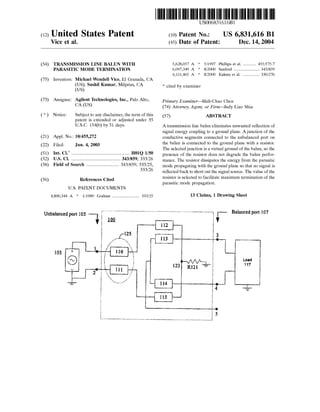
Unbalanced port 105 ' """"""""" t Balanced port 107
l m 4112
125
1 13 i
J: 1 ,1". .
103 + _; H0
@ W Load_ 123 R121 —_—- 117
t 2
111d? ~'>“~~..._..~.,.->"v‘ l ‘
4 4;
115
O
5
3. US 6,831,616 B1
1
TRANSMISSION LINE BALUN WITH
PARASITIC MODE TERMINATION
BACKGROUND OF THE INVENTION
A transmission line balun is a passive device used as an
interface betWeen a balanced network and an unbalanced
network. The balun is commonly used to convert an unbal
anced radio frequency (RF) signal source to a balanced
signal. HoWever, a problematic side effect of this conversion
involves unavoidable coupling betWeen the balun and a
nearby ground plane. This phenomenon Will be referred to as
parasitic mode propagation.
In parasitic mode propagation, some of the energy from
the RF signal source propagates betWeen the balun and the
ground plane. A narroWband disappearance in frequency
response, knoWn as a suckout, occurs at signal frequencies
in Which the balun has an effective electrical length of
(2N+1)90° betWeen the unbalanced port and the balanced
port, Where N is any integer. At these frequencies, the RF
signal source is effectively shorted to ground and causes a
narroWband suckout.
Prior art solutions adjusted the length of the conductive
segments Within the balun to shift the suckout outside the
frequency band of interest. HoWever, changing the segment
lengths can cause the phase performance, match loss, and/or
insertion loss of the balun to suffer. Furthermore, the suckout
is only shifted to a different frequency band—it is not
completely eliminated.
SUMMARY OF THE INVENTION
In accordance With a preferred embodiment of the present
invention, a junction betWeen the conductive segments
connected to the unbalanced port on the balun is connected
to ground With a resistor to eliminate suckout due to parasitic
mode propagation. The selected junction is a virtual ground
of the balun, so the presence of the resistor does not degrade
the balun performance. The resistor dissipates the energy
from the unWanted signal coupling due to parasitic mode
propagation, thus preventing the 90 degree phase delay that
Would short out the RF signal source. The value of the
resistor is selected to facilitate maXimum termination of the
parasitic mode propagation. With all of the parasitic mode
propagation terminated, no undesired re?ection of energy
can occur and the narroWband short circuit seen at the input
is completely eliminated.
Further features and advantages of the present invention,
as Well as the structure and operation of preferred embodi
ments of the present invention, are described in detail beloW
With reference to the accompanying exemplary draWings. In
the draWings, like reference numbers indicate identical or
functionally similar segments.
BRIEF DESCRIPTION OF THE DRAWINGS
FIG. 1 shoWs a schematic of a preferred embodiment of
a balun, made in accordance With the teachings of the
present invention.
DETAILED DESCRIPTION
FIG. 1 shoWs a schematic of a preferred embodiment of
a balun 100, made in accordance With the teachings of the
present invention. The balun 100 converts an unbalanced
signal from a radio frequency (RF) signal source 103 to a
balanced signal. The balun 100 has an unbalanced port 105
for input from an RF signal source 103 and a balanced port
10
15
25
35
40
45
55
65
2
107 for output of the balanced signal. The unbalanced port
105 consists of terminals 1 and 2. The balanced port 107
consists of terminals 3, 4, and 5. The balanced port 107 is
connected to a load 117.
Conductive segments 110, 112, 115, and 11 are connected
in series betWeen terminal 1 and terminal 2, respectively.
The junction betWeen conductive segments 112 and 115 is
designated node 123. Conductive segments 113 and 114 are
connected in series betWeen terminal 3 and terminal 4,
respectively. The junction betWeen conductive segments 113
and 114 is designated as terminal 5.
Conductive segments 110 and 111 form an electromag
netically coupled pair, and preferably have equal lengths and
equal Widths. Conductive segments 110 and 111 function as
an isolation transformer 125. The isolation transformer 125
is preferably used to isolate the balanced signal from ground,
but it is not absolutely necessary to the performance of the
balun 100. Conductive segments 112 and 113 form another
electromagnetically coupled pair, and so do conductive
segments 114 and 115. Conductive segments 112, 113, 114,
and 115 preferably have equal lengths and equal Widths.
To convert the single-ended RF signal source 103 to a
balanced signal, one terminal of the RF signal source 103 is
connected to terminal 1, While its other terminal is connected
to terminal 2 and grounded. An unbalanced signal applied to
the unbalanced port 105 produces a balanced signal at the
balanced port 107, by virtue of the electromagnetic coupling
betWeen the conductive segments. Assuming the load 117
has symmetric impedance With respect to ground, the con
ductive segments are arranged so that the signals at termi
nals 3 and 4 are equal in amplitude With respect to ground,
but have a 180° phase difference. As a result, both node 123
and terminal 5 are virtual grounds of the balun 100. Terminal
5 may be grounded to enforce ground centering at the
balanced port 107, left ?oating as a virtual ground, or
connected to another circuit eXternal to the balun 100. The
selection of materials and the design of the conductive
segments are Well knoWn to those skilled in the art.
The lengths and Widths of all the conductive segments, as
Well as the separation betWeen the electromagnetically
coupled pairs, are preferably selected to match the charac
teristic impedance of the RF signal source 103 over the
frequency band of interest. Terminals 3 and 4 are connected
to a load 117. The balun 100 is typically used in a system
Where the source and load impedances are the same, but this
need not alWays the case.
Previously, the RF signal source 103 Would be substan
tially shorted to ground at frequencies at Which the balun has
an effective electrical length of (2N+1)90° betWeen terminal
1 and node 123 for the parasitic mode. To prevent this, a
resistor R121 connects node 123 to ground. The resistor
R121 dissipates the energy from the parasitic mode propa
gation so that virtually Zero signal is re?ected back to short
out the RF signal source 103. The presence of the resistor
R121 does not degrade the balun performance since node
123 is a virtual ground of the balun 100. The value of the
resistor R121 is selected to facilitate maXimum termination
of the parasitic mode propagation arriving at node 123. With
most of the parasitic mode propagation terminated at node
123, little or no undesired re?ection of energy can occur and
the narroWband suckout is essentially eliminated.
The value of resistor R121 matches the characteristic
impedance of the parasitic mode propagation betWeen the
balun 100 and the ground plane. This value depends prima
rily on the Width of the conductive segments, the dielectric
material separating the balun 100 from the ground plane, and
4. US 6,831,616 B1
3
the distance between the balun 100 and the ground plane.
The appropriate value can be determined empirically or
through circuit simulation.
Those With skill in the art Will recognize that the balun
may be implemented in multiple forms, including: stripline,
microstrip, tWisted pair, coaXial cables, multi?lar Wire, etc.
The balun may also be used to convert balanced signals to
unbalanced ones by attaching a signal source at the balanced
port 107 and taking the output from the unbalanced port 105.
Although the present invention has been described in
detail With reference to particular preferred embodiments,
persons possessing ordinary skill in the art to Which this
invention pertains Will appreciate that various modi?cations
and enhancements may be made Without departing from the
spirit and scope of the claims that folloW.
We claim:
1. A balun, comprising:
an unbalanced port comprising a ?rst and second termi
nal;
a balanced port comprising a third, fourth, and ?fth
terminal;
?rst and second conductive segments respectively con
nected in series betWeen the ?rst and second terminal;
third and fourth conductive segments respectively con
nected in series betWeen the third and fourth terminal,
the junction betWeen the third and fourth conductive
segments comprising the ?fth terminal,
Wherein the ?rst and third conductive segments form an
electromagnetically coupled pair, and the second and
fourth conductive segments form an electromagneti
cally coupled pair;
a ground plane; and
a resistor connecting the junction betWeen the ?rst and
second conductive segments to the ground plane.
2. The balun as in claim 1, Wherein the resistor value is
selected so as to substantially eliminate unWanted re?ection
15
25
35
4
of signal energy in the parasitic mode propagating betWeen
the balun and the ground plane.
3. The balun as in claim 2, further comprising an isolation
transformer interposing the unbalanced port and the ?rst and
second conductive segments.
4. The balun as in claim 3, Wherein the ?rst, second, third,
and fourth conductive segments have equal lengths and
equal Widths.
5. The balun as in claim 4, Wherein the ?fth terminal is
connected to ground.
6. The balun as in claim 5, Wherein the isolation trans
former comprises:
?fth and siXth conductive segments having equal lengths
and equal Widths that form an electromagnetically
coupled pair.
7. The balun as in claim 1, further comprising an isolation
transformer interposing the unbalanced port and the ?rst and
second conductive segments.
8. The balun as in claim 7, Wherein the ?rst, second, third,
and fourth conductive segments have equal lengths and
equal Widths.
9. The balun as in claim 8, Wherein the ?fth terminal is
connected to ground.
10. The balun as in claim 9, Wherein the isolation trans
former comprises:
?fth and siXth conductive segments having equal lengths
and equal Widths that form an electromagnetically
coupled pair.
11. The balun as in claim 1, Wherein the ?rst, second,
third, and fourth conductive segments have equal lengths
and equal Widths.
12. The balun as in claim 11, Wherein the resistor value is
selected so as to substantially eliminate unWanted re?ection
of signal energy in the parasitic mode propagating betWeen
the balun and the ground plane.
13. The balun as in claim 12, Wherein the ?fth terminal is
connected to ground.