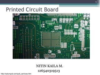
3. Printed Circuit Board
Circuit connects components through board
Made of alternating layers of conducting and
insulating materials
3
http://www.seilpcb.co.kr/products/images/2_1_img5.gif
4. Why PCB?
• Features
• Surprisingly Affordable
• Highly reliable
• Compact
• Drawbacks
• Requires more layout than other board types
• Higher initial cost than wire wrap or point-to-
point construction
4
http://en.wikipedia.org/wiki/File:Breadboard_complex.jpg
5. PCB Design Steps
1 Design the circuit
2 Place the components
3 Route the wires
4 Manufacture
5
6. EDA Software
• PCB design software package
• Design the circuit (Schematics editor)
• Place the components (PCB editor)
• Route the wires (Autorouter module)
• Examples:
• EAGLE
• ExpressPCB
6
9. Placement of Components
• Place big components first- e.g. microcontroller
• Place components in separate functional groups
• Put a ground plane under all components
9
10. Signal Routing Component Placement
• Surface mount
• Top and bottom planes
• Minimal routing area
• Through-hole mounted
• All components on same side
• Reduces routing area on all planes
10
http://www.ehow.com/how_8306661_solder-mini-components.html
http://blog.amal.net/?p=188
11. Signal Routing
• Traces are wires connecting components
• Traces can be routed through multiple layers
11
12. Vias and Pads
• Vias are connections between layers
• Pads are copper areas for pin connections
12
13. Manufacturing Files
• Gerber Files
• Industry standard file format to describe circuits
• Generated by PCB design software
• Contains all necessary info to manufacture a
circuit board (Traces, Pads, Silkscreen, etc.)
• Drill Files
• Describes the location and size of holes
• Zipped with Gerber files and sent to manufacturer
13
17. Summary
• PCBs allow for portable and reliable circuits
• Designed in EDA Software
▫ Design the circuit
▫ Place the components
▫ Route the wires
▫ Manufacture
• Price varies based on size and urgency
17