2. 3.Oxide Growth & Removal
a) Oxide Growth & Deposition
b) Oxide Removal
c) Other effects
d) Local Oxidation
4. Diffusion & Ion Implantation
a) Diffusion
b) Other effects
c) Ion Implantation
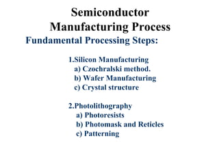
Semiconductor Manufacturing
Process (cont)
4. FABRICATING SILICON
Quartz, or Silica, Consists of Silicon Dioxide
Sand Contains Many Tiny Grains of Quartz
Silicon Can be Artificially Produced by
Combining Silica and Carbon in Electric
Furnice
Gives Polycrystalline Silicon (multitude of
crystals)
Practical Integrated Circuits Can Only be
Fabricated from Single-Crystal Material
5. CRYSTAL GROWTH
Czochralski Process
is a Technique in
Making Single-Crystal
Silicon
A Solid Seed Crystal
is Rotated and Slowly
Extracted from a Pool
of Molten Si
Requires Careful
Control to Give
Crystals Desired
Purity and
Dimensions
6. CYLINDER OF
MONOCRYSTALLINE
The Silicon Cylinder is
Known as an Ingot
Typical Ingot is About 1
or 2 Meters in Length
Can be Sliced into
Hundreds of Smaller
Circular Pieces Called
Wafers
Each Wafer Yields
Hundreds or Thousands
of Integrated Circuits
7. WAFER MANUFACTURING
The Silicon Crystal is Sliced by Using a Diamond-Tipped Saw
into Thin Wafers
Sorted by Thickness
Damaged Wafers Removed During Lapping
Etch Wafers in Chemical to Remove any Remaining Crystal
Damage
Polishing Smoothes Uneven Surface Left by Sawing Process
10. Photolithography
Photoresist
The first step in the photolithography process is to
develop a mask, which will be typically be a
chromium pattern on a glass plate.
Next, the wafer is then coated with a polymer
which is sensitive to ultraviolet light called a
photoresist.
Afterward, the photoresist is then developed which
transfers the pattern on the mask to the
photoresist layer.
12. Photolithography
Photoresist
There are two basic types of Photoresists Positive and Negative.
Positive resists.
Positive resists decomposes ultraviolet light. The resist is
exposed with UV light wherever the underlying material is to be
removed. In these resists, exposure to the UV light changes the
chemical structure of the resist so that it becomes more soluble in
the developer. The exposed resist is then washed away by the
developer solution, leaving windows of the bare underlying
material. The mask, therefore, contains an exact copy of the
pattern which is to remain on the wafer.
13. Photolithography
Photoresist
Negative resists
Exposure to the UV light causes the negative resist to become
polymerized, and more difficult to dissolve. Therefore, the
negative resist remains on the surface wherever it is exposed, and
the developer solution removes only the unexposed portions.
Masks used for negative photoresists, therefore, contain the
inverse (or photographic "negative") of the pattern to be
transferred.
14. Photolithography
Model
Figure 1a shows a thin film
of some material (eg,
silicon dioxide) on a
substrate of some other
material (eg, a silicon
wafer).
Photoresist layer (Figure
1b )
Ultraviolet light is then
shone through the mask
onto the photoresist
(figure 1c).
15. Photolithography
Model (cont)
The photoresist is then
developed which transfers
the pattern on the mask to
the photoresist layer (figure
1d).
A chemical (or some other
method) is then used to
remove the oxide where it
is exposed through the
openings in the resist
(figure 1e).
Finally the resist is
removed leaving the
patterned oxide (figure 1f).
16. Photolithography
Photomasks and Reticles
Photomask
This is a square glass plate with a patterned emulsion of metal film
on one side. The mask is aligned with the wafer, so that the pattern
can be transferred onto the wafer surface. Each mask after the first
one must be aligned to the previous pattern.
17. Photolithography
Photomasks and Reticles
When a image on the photomask is projected several time side by side onto
the wafer, this is known as stepping and the photomask is called a reticle.
An common reticle is the 5X
The patterns on the 5X reticle are reduced 5 times when
projected onto the wafer. This means the dies on the
photomask are 5 times larger than they are on the final
product. There are other kinds of reduction reticles (2X, 4X,
and 10X), but the 5X is the most commonly used. Reduction
reticles are used on a variety of steppers, the most common
being ASM, Canon, Nikon, and GCA.