

Recommended
More Related Content
What's hot
What's hot (20)
Viewers also liked
Viewers also liked (20)
Similar to TRANSISTORS
Similar to TRANSISTORS (20)
More from AJAL A J
More from AJAL A J (20)
Recently uploaded
Recently uploaded (20)
TRANSISTORS
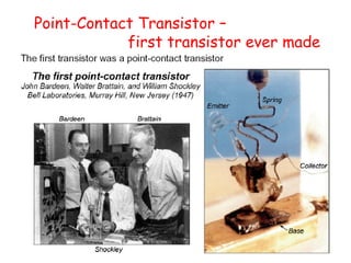
- 1. Point-Contact Transistor – first transistor ever made
- 2. The Wonder child of electronics By AJAL.A.J ( ASSISTANT PROFESSOR) ECE DEPARTMENT MAIL: ec2reach@gmail.com MOB: 8907305642
- 3. What is a transistor? A transistor is a 3 terminal electronic device made of semiconductor material. Transistors have many uses, including amplification, switching, voltage regulation, and the modulation of signals
- 4. This session will help you to understand the, 1.Evolution of transistor 2.Importance of transistor 3.Definition & transistor types 4.Transistor symbol & operation 5.Advantages of transistor 6.Latest in transistor technology
- 5. History of transistors In 1906, an American inventor and physicist, Lee De Forest, made the vacuum tube triode or audion as he called it. Used in radios Used in early computers
- 6. Interesting story… Picture shows the workbench of John Bardeen (Stocker Professor at OU) and Walter Brattain at Bell Laboratories. They were supposed to be doing fundamental research about crystal surfaces. The experimental results hadn't been very good, though, and there's a rumor that their boss, William Shockley, came near to canceling the project. But in 1947, working alone, they switched to using tremendously pure materials. It dawned on them that they could build the circuit in the picture. It was a working amplifier! John and Walter submitted a patent for the first working point contact transistor.
- 7. Interesting story… Shockley was furious and took their work and invented the junction transistor and submitted a patent for it 9 days later. The three shared a Nobel Prize in 1955. Bardeen and Brattain continued in research (and Bardeen later won another Nobel). Shockley quit to start a semiconductor company in Palo Alto. It folded, but its staff went on to invent the integrated circuit (the "chip") and to found Intel Corporation. By 1960, all important computers used transistors for logic, and ferrite cores for memory.
- 9. Qualitative basic operation of point-contact transistor Problems with first transistor…
- 10. First Bipolar Junction Transistors W. Shockley invented the p-n junction transistor The physically relevant region is moved to the bulk of the material
- 11. Moore’s Law It’s an observation made by Gordon E. Moore, in which he predicted that the number of transistors, inside an Integrated Circuit, could be doubled every 24 months. At the density that also minimized the cost of a transistor.
- 12. Transistor Definition Transistor is an electronic device made of three layers of semiconductor material that can act as an insulator and a conductor. The three layered transistor is also known as the bipolar junction transistor.
- 13. Basic models of BJT
- 14. BJTs – Basic Configurations pnp BJT npn BJT
- 15. Bipolar Junction Transistors (BJT’s) The term bipolar refers to the use of both holes and electrons as charge carriers in the transistor structure There are two types of BJTs, the NPN and PNP
- 16. Origin of the names the Emitter 'emits' the electrons which pass through the device the Collector 'collects' them again once they've passed through the Base ...and the Base?...
- 17. Transistor operation force – voltage/current water flow – current - amplification
- 18. Architecture of BJTs The bipolar junction transistor (BJT) is constructed with three doped semiconductor regions separated by two pn junctions Regions are called emitter, base and collector
- 20. Architecture of BJTs There are two types of BJTs, the npn and pnp The two junctions are termed the base-emitter junction and the base-collector junction The term bipolar refers to the use of both holes and electrons as charge carriers in the transistor structure In order for the transistor to operate properly, the two junctions must have the correct dc bias voltages the base-emitter (BE) junction is forward biased(>=0.7V for Si, >=0.3V for Ge) the base-collector (BC) junction is reverse biased
- 21. Regions of a transistor A transistor has three regions namely, Emitter- heavily doped Base- lightly doped Collector- moderately doped
- 22. Transistor symbols Transistor symbols
- 25. How does IC vary with VCE for various IB? Note that both dc sources are variable Set VBB to establish a certain IB
- 26. Transistor biasing The base-emitter (BE) junction is forward biased The base-collector (BC) junction is reverse biased. IE=IB+IC
- 27. • Output current can toggle between large and small (Switching Digital logic; create 0s and 1s)
- 28. Operating regions of BJT Cut off region Linear region Saturation region
- 29. Types of transistor BJT - Bipolar Junction Transistor UJT- Unipolar Junction Transistor FET - Field Effect Transistor MOS - Metal Oxide Semiconductor
- 30. Basic circuits of BJT
- 31. Operation of BJTs BJT will operates in one of following four region Cutoff region (for digital circuit) Saturation region (for digital circuit) Linear (active) region (to be an amplifier) Breakdown region (always be a disaster)
- 33. DC Analysis of BJTs Transistor Currents: IE = IC + IB alpha (aDC) IC = aDCIE beta (bDC) IC = bDCIB bDC typically has a value between 20 and 200
- 34. DC Analysis of BJTs DC voltages for the biased transistor: Collector voltage VC = VCC - ICRC Base voltage VB = VE + VBE for silicon transistors, VBE = 0.7 V for germanium transistors, VBE = 0.3 V
- 35. Q-point The base current, IB, is established by the base bias The point at which the base current curve intersects the dc load line is the quiescent or Q-point for the circuit
- 36. Q-point
- 37. DC Analysis of BJTs The voltage divider biasing is widely used Input resistance is: RIN @ bDCRE The base voltage is approximately: VB @ VCCR2/(R1+R2)
- 38. BJT as an amplifier Class A Amplifiers Class B Amplifiers
- 40. BJT Class A Amplifiers In a class A amplifier, the transistor conducts for the full cycle of the input signal (360°) used in low-power applications The transistor is operated in the active region, between saturation and cutoff saturation is when both junctions are forward biased the transistor is in cutoff when IB = 0 The load line is drawn on the collector curves between saturation and cutoff
- 41. BJT Class A Amplifiers
- 42. BJT Class A Amplifiers Three biasing mode for class A amplifiers common-emitter (CE) amplifier common-collector (CC) amplifier common-base (CB) amplifier
- 43. BJT Class A Amplifiers A common-emitter (CE) amplifier capacitors are used for coupling ac without disturbing dc levels
- 44. BJT Class A Amplifiers A common-collector (CC) amplifier voltage gain is approximately 1, but current gain is greater than 1
- 45. BJT Class A Amplifiers BJT Class A Amplifiers The third configuration is the common-base (CB) the base is the grounded (common) terminal the input signal is applied to the emitter output signal is taken off the collector output is in-phase with the input voltage gain is greater than 1 current gain is always less than 1
- 46. BJT Class B Amplifiers
- 47. BJT Class B Amplifiers When an amplifier is biased such that it operates in the linear region for 180° of the input cycle and is in cutoff for 180°, it is a class B amplifier A class B amplifier is more efficient than a class A In order to get a linear reproduction of the input waveform, the class B amplifier is configured in a push-pull arrangement The transistors in a class B amplifier must be biased above cutoff to eliminate crossover distortion
- 49. The BJT as a Switch When used as an electronic switch, a transistor normally is operated alternately in cutoff and saturation A transistor is in cutoff when the base-emitter junction is not forward-biased. VCE is approximately equal to VCC When the base-emitter junction is forward-biased and there is enough base current to produce a maximum collector current, the transistor is saturated
- 50. The BJT as a Switch
- 51. An example -- NOR
- 52. Transistor applications Transistor as a switch When used as an electronic switch, the transistor is normally operated alternately in cut-off and saturation regions.
- 53. Transistor as amplifier Due to the small changes in base current the collector current will mimic the input with greater amplitude
- 54. Future of Transistors Molecular electronics Carbon nanotube transistors Nano inspiration wire transistors Quantum computing CMOS devices will add functionality to CMOS non-volatile memory, opto-electronics, sensing…. CMOS technology will address new markets macroelectronics, bio-medical devices, … Biology may provide for new technologies bottom-up assembly, human intelligence
- 55. What’s new in transistor technology? 3D Transistor made using Tri-Gate transistors on its 22nm logic technology. Advantage of Tri-Gate Transistors ·More than 50% power reduction at constant performance. ·37% performance increase at low voltage ·Improved performance and efficiency.
- 56. BJTs – Practical Aspects
- 57. BJTs – Practical Aspects Heat sink
- 58. BJTs – Testing
- 59. BJTs – Testing