ECE 468 Lab Project 1
•Download as DOCX, PDF•
0 likes•316 views

Full wave Rectifier using Hspice

Recommended
More Related Content
Viewers also liked
Viewers also liked (13)
Similar to ECE 468 Lab Project 1
Similar to ECE 468 Lab Project 1 (20)
More from Lakshmi Yasaswi Kamireddy
Recently uploaded
Recently uploaded (20)
ECE 468 Lab Project 1
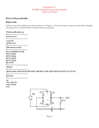
- 1. Experiment 1 NAME: Lakshmi Yasaswi Kamireddy UIN: 651771619 Part I – Full wave Rectifier Hspice code: Netlist is created according to the node numbers as in Figure 1. Values for output voltage are obtained by changing the parameters as required. Model of diode is taken as specified. *FullwaveRectifier.sp *--------------------------------- *Parameters *--------------------------------- .temp 20 .option post *--------------------------------- *Simulation netlist *--------------------------------- Vin 1 0 SIN(0V 5V 50) D1 0 1 diode D3 0 2 diode D4 1 3 diode D2 2 3 diode R1 3 0 50 *--------------------------------- *Model *--------------------------------- .Model diode D(IS=18.8n RS=0 BV=400 IBV=5.00u CJO=30 M=0.333N=2.0 TT=0) *--------------------------------- Stimulus *--------------------------------- .op .tran .01m 1m .print V(3,0) .end Figure 1 3
- 2. Observations: Figure 2 shows the output and input when temperature = 20 degree, Frequency = 50 Hz, Ideality Factor =2. Red shows the Input and blue shows the output. The maximum Output voltage obtained with an ideality factor of 2 is 2.6212 which is very less than 3.6 (Vin-1.4). As the ideality factor decreases to 1 the output voltage increases as seen in Figure 3. The maximum value obtained is 3.823V when the idealityfactor is 1. Also we can see that the output voltage increases with each cycle. Figure 25 shows that with increase in temperature the output voltage decreases. Results: Q: 3, 4, 5 Figure 2 Figure 3 -6 -4 -2 0 2 4 6 0 5 10 15 20 25 30 35 40 45 50 55 60 65 70 75 80 85 90 95 100 VOLTAGE()V Temp-20,Frequency-50,N=2 N=2 INPUT VOLTAGE 0 1 2 3 4 5 1 6 11 16 21 26 31 36 41 46 51 56 61 66 71 76 81 86 91 96 101 Voltage Time(ms) Temp-20,Frequency-50 N=2 N=1.75 N=1.5 N=1.25 N=1
- 3. Figure 4 Figure 5 Figure 6 -6 -4 -2 0 2 4 6 0 5 10 15 20 25 30 35 40 45 50 55 60 65 70 75 80 85 90 95 100 VOLTAGE(V) TIME(MILLI SECONDS) Temp=20,Frequency=60Hz,N=2 N=2 INPUT VOLTAGE 0 0.5 1 1.5 2 2.5 3 3.5 4 1 5 9 13 17 21 25 29 33 37 41 45 49 53 57 61 65 69 73 77 81 85 89 93 97 101 105 Voltage(V) Time(ms) Temp=20,Frequency=60Hz N=2 N=1.75 N=1.5 N=1 -6 -4 -2 0 2 4 6 0 4 8 12 16 20 24 28 32 36 40 44 48 52 56 60 64 68 72 76 80 84 88 92 96 100 VOLTAGE TIME(MS) Temp=20,Frequency=70Hz,N=2 N=2 INPUT VOLTAGE
- 4. Figure 7 Figure 8 Figure 9 0 0.5 1 1.5 2 2.5 3 3.5 4 1 5 9 13 17 21 25 29 33 37 41 45 49 53 57 61 65 69 73 77 81 85 89 93 97 101 Voltage Time(ms) Temp=20,Frequency=70 N=2 N=1.75 N=1.5 N=1 -6 -4 -2 0 2 4 6 0 4 8 12 16 20 24 28 32 36 40 44 48 52 56 60 64 68 72 76 80 84 88 92 96 100 VOLTAGE TIME(MILLI SECONDS) Temp 30,Frequency=50Hz,N=2 N=2 INPUT VOLTAGE 0 1 2 3 4 5 1 5 9 13 17 21 25 29 33 37 41 45 49 53 57 61 65 69 73 77 81 85 89 93 97 101 Voltage Time(ms) Temp=30,Frequency=50 N=2 N=1.75 N=1.5 N=1
- 5. Figure 10 Figure 11 Figure 12 -6 -4 -2 0 2 4 6 0 3 6 9 12151821242730333639424548515457606366697275788184879093 VOLTAGE TIME(MILLI SECOND) Temp=30,Frequency=60Hz,N=2 N=2 INPUT VOLTAGE 0 0.5 1 1.5 2 2.5 3 3.5 4 4.5 1 5 9 13 17 21 25 29 33 37 41 45 49 53 57 61 65 69 73 77 81 85 89 93 97 101 Voltage Time(ms) Temp=30,Frequency=60 N=2 N=1.75 N=1.5 N=1 -6 -4 -2 0 2 4 6 0 4 8 12 16 20 24 28 32 36 40 44 48 52 56 60 64 68 72 76 80 84 88 92 96 100 VOLTAGE TIME(MILLI SECOND) Temp=30,Frequency=70Hz N=2 INPUT VOLTAGE
- 6. Figure 13 Figure 14 Figure 15 0 0.5 1 1.5 2 2.5 3 3.5 4 4.5 1 5 9 13 17 21 25 29 33 37 41 45 49 53 57 61 65 69 73 77 81 85 89 93 97 101 Voltage Time(ms) Temp=30,Frequency=70Hz N=2 N=1.75 N=1.5 N=1 -6 -4 -2 0 2 4 6 0 4 8 12 16 20 24 28 32 36 40 44 48 52 56 60 64 68 72 76 80 84 88 92 96 100 VOLATGE TIME(MILLI SECOND) Temp=40,Frequency=50,N=2 N=2 INPUT VOLTAGE 0 1 2 3 4 5 1 5 9 13 17 21 25 29 33 37 41 45 49 53 57 61 65 69 73 77 81 85 89 93 97 101 Voltage Time(ms) Temp=40,Frequency=50 N=2 N=1.75 N=1.5 N=1
- 7. Figure 15 Figure 16 Figure 17 -6 -4 -2 0 2 4 6 0 4 8 12 16 20 24 28 32 36 40 44 48 52 56 60 64 68 72 76 80 84 88 92 96 100 VOLTAGE TIME(MILLI SECOND) Temp=40,Frequency=60Hz,N=2 N=2 INPUT VOLTAGE 0 0.5 1 1.5 2 2.5 3 3.5 4 4.5 1 5 9 13 17 21 25 29 33 37 41 45 49 53 57 61 65 69 73 77 81 85 89 93 97 101 Voltage Time(ms) Temp=40,Frequency=60Hz N=2 N=1.75 N=1.5 N=1 -6 -4 -2 0 2 4 6 0 4 8 12 16 20 24 28 32 36 40 44 48 52 56 60 64 68 72 76 80 84 88 92 96 100 VOLATGE TIME(MIILI SECOND) Temp=40,Frequency=70Hz,N=2 N=2 INPUT VOLTAGE
- 8. Figure 18 Figure 19 Figure 20 0 0.5 1 1.5 2 2.5 3 3.5 4 4.5 1 5 9 13 17 21 25 29 33 37 41 45 49 53 57 61 65 69 73 77 81 85 89 93 97 101 Voltage Time(ms) Temp=40,Frequency=70Hz N=2 N=1.75 N=1.5 N=1 -6 -4 -2 0 2 4 6 0 4 8 12 16 20 24 28 32 36 40 44 48 52 56 60 64 68 72 76 80 84 88 92 96 100 VOLTAGE TIME(MILLI SECOND) Temp=50,Frequency=50Hz,N=2 N=2 INPUT VOLTAGE 0 1 2 3 4 5 1 5 9 13 17 21 25 29 33 37 41 45 49 53 57 61 65 69 73 77 81 85 89 93 97 101 Volatge Time(ms) Temp=50,Frequency=50hz N=2 N=1.75 N=1.5 N=1
- 9. Figure 21 Figure 22 Figure 23 -6 -4 -2 0 2 4 6 0 4 8 12 16 20 24 28 32 36 40 44 48 52 56 60 64 68 72 76 80 84 88 92 96 100 VOLTAGE TIME(MILLI SECOND) Temp=50,Frequency=60Hz,N=2 N=2` INPUT VOLTAGE 0 0.5 1 1.5 2 2.5 3 3.5 4 4.5 1 5 9 13 17 21 25 29 33 37 41 45 49 53 57 61 65 69 73 77 81 85 89 93 97 101 Voltage Time(ms) Temp=50,Frequency=60Hz N=2` N=1.75 N=1.5 N=1 -6 -4 -2 0 2 4 6 0 4 8 12 16 20 24 28 32 36 40 44 48 52 56 60 64 68 72 76 80 84 88 92 96 100 VOLTAGE TIME(MS) Temp=50,Frequency=70Hz,N=2 N=2 INPUT VOLTAGE
- 10. Figure 24 Figure 25 Part II – MOSFET Characteristics Hspice code: *Mosfetidvds.sp *NMOS Id - Vgs Characteristics--------------- *-------------------------------------------- *Paramters *-------------------------------------------- .option post *-------------------------------------------- *Simulation netlist *-------------------------------------------- Vds 1 0 DC 5V Vgs 2 0 DC 5V M1 1 2 0 0 nmos1 L=2.5u W=2.5u *--------------------------------------------- 0 0.5 1 1.5 2 2.5 3 3.5 4 4.5 1 5 9 13 17 21 25 29 33 37 41 45 49 53 57 61 65 69 73 77 81 85 89 93 97 101 Voltage Time(ms) Temp=50,Frequency=70Hz N=2 N=1.75 N=1.5 N=1 0 0.5 1 1.5 2 2.5 3 0 1 2 3 4 5 6 7 8 9 10 11 12 13 14 15 16 17 18 19 20 Voltage Time(ms) Frequency=50Hz,N=2 Temp=20 Temp=30 Temp=40 Temp=50
- 11. *Model *--------------------------------------------- .model nmos1 nmos (LEVEL=3 RSH=0 TOX=300E-10 LD=0.21E-6 XJ=0.3E-6 +VMAX=15E4 ETA=0.18 GAMMA=0.4 KAPPA=0.5 NSUB=35E14 UO=700 +THETA=0.095 VTO=0.781 CGSO=2.8E-10 CGDO=2.8E-10 +CJ=5.75E-5 CJSW=2.48E-10 PB=0.7 MJ=0.5 MJSW=0.3 NFS=1E10) *---------------------------------------------- *Stimulus *---------------------------------------------- .DC Vgs 0V 5V 100mV .print DC I(M1) .end *Mosfetidvds.sp *NMOS Id - Vds Characteristics--------------- *-------------------------------------------- *Paramters *-------------------------------------------- .option post *-------------------------------------------- *Simulation netlist *-------------------------------------------- Vds 1 0 DC 5V Vgs 2 0 DC 2V M1 1 2 0 0 nmos1 L=2.5u W=2.5u *--------------------------------------------- *Model *--------------------------------------------- .model nmos1 nmos (LEVEL=3 RSH=0 TOX=300E-10 LD=0.21E-6 XJ=0.3E-6 +VMAX=15E4 ETA=0.18 GAMMA=0.4 KAPPA=0.5 NSUB=35E14 UO=700 +THETA=0.095 VTO=0.781 CGSO=2.8E-10 CGDO=2.8E-10 +CJ=5.75E-5 CJSW=2.48E-10 PB=0.7 MJ=0.5 MJSW=0.3 NFS=1E10) *---------------------------------------------- *Stimulus *---------------------------------------------- .DC Vds 0V 5V 100mV .print DC I(M1) .end Changing value of Vgs and resimulating. An alternate way is to put Vgs also to DC sweep. Observations: Q : 4, 5, 6, 7 and Question 1,2 From Figure 26: When Vgs=0V the Id value is almost 0. That means the mosfet is in cutoff region. When Vgs>Vth say Vgs=5V until Vgs-Vth>Vds i.e approximately until Vds=4.3 the mosfet is in linear region and hence Id is proportional to Vds^2. When Vgs-Vth<Vds the mosfet enters to saturation and the current becomes constant with respect to Vds. This can be supported by the equations below:
- 12. From Figure 27: When Vgs<Vth value of Id is almost 0 When Vgs > Vth say 0.7 V value of Id increases with Vgs. From Figure 28: The region below Vgs=0.7(threshold volatge) is the cutoff region. The first half of the intersection of the Id-Vgs and Id-Vds curve is the linear region and the second half is the saturation region. Figure 26 Figure 27 0 50 100 150 200 250 300 350 400 450 0 0.20.40.60.8 1 1.21.41.61.8 2 2.22.42.62.8 3 3.23.43.63.8 4 4.24.44.64.8 5 Id(uA) Vds(V) Id vs Vds for differentVgs Vgs=0V Vgs=1V Vgs=2V Vgs=3V Vgs=4V Vgs=5V 0 50 100 150 200 250 300 350 400 450 0 0.20.40.60.8 1 1.21.41.61.8 2 2.22.42.62.8 3 3.23.43.63.8 4 4.24.44.64.8 5 Id(uA) Vgs(V) Id vs Vgs for Vds=5V
- 13. Figure 28 Conclusions: The experiment was performed successfully and it is found that the values obtained from the simulations match with the theoretical values. Appendix: Sample Data for Full Wave Rectifier – each column represents the output voltage for the value of ideality factor. temp= 20 freq=50 time voltage N=2 INPUT VOLTAGE N=1.75 N=1.5 N=1.25 N=1 0 0 0 0 0 0 0 1 202.7935 0.2027935 2.1289 0.2027936 0.2027947 0.202827 0.20743 2 635.566 0.635566 3.8441 0.6507013 0.7899721 1.1339 1.4831 3 1.2419 1.2419 4.8339 1.5664 1.9165 2.2663 2.6154 4 1.9714 1.9714 4.9114 2.3229 2.6602 3.0028 3.353 5 2.3216 2.3216 4.0451 2.6602 2.9967 3.3328 3.6648 6 2.2739 2.2739 2.4082 2.6085 2.9412 3.2726 3.6013 7 1.9734 1.9734 0.3136172 2.3166 2.6586 3.0012 3.3429 8 1.5601 1.5601 -1.8384 1.9216 2.2852 2.6499 3.0176 9 1.1849 1.1849 -3.6428 1.5755 1.9694 2.368 2.7649 10 1.0307 1.0307 -4.7546 1.4417 1.8532 2.2643 2.6709 11 1.1852 1.1852 -4.9604 1.5768 1.9718 2.371 2.765 12 1.5602 1.5602 -4.2171 1.9218 2.2842 2.6507 3.0215 13 1.9735 1.9735 -2.6783 2.3166 2.6586 3.0012 3.3429 14 2.2847 2.2847 -0.6197 2.616 2.9454 3.2741 3.6022 15 2.4325 2.4325 1.5439 2.757 3.0791 3.3998 3.7191 16 2.3464 2.3464 3.4225 2.6727 2.9953 3.3169 3.637 17 2.0467 2.0467 4.6482 2.3806 2.7138 3.0468 3.3799 18 1.6375 1.6375 4.9901 1.9892 2.3429 2.6998 3.0575 19 1.2941 1.2941 4.3701 1.648 2.0338 2.421 2.8074 0 100 200 300 400 500 0 0.20.40.60.8 1 1.21.41.61.8 2 2.22.42.62.8 3 3.23.43.63.8 4 4.24.44.64.8 5 Id(uA) Volt(V) Id for Vgs and Vds varying from0 to 5V Vgs=0V Vgs=1V Vgs=2V Vgs=3V Vgs=4V Vgs=5V Vds=5V
- 14. 20 1.1182 1.1182 2.9372 1.5186 1.9196 2.3188 2.7145 21 1.2736 1.2736 0.9193783 1.6507 2.0378 2.4216 2.8121 22 1.6416 1.6416 -1.2418 1.9913 2.3457 2.7004 3.0603 23 2.0467 2.0467 -3.1744 2.3806 2.7138 3.0468 3.3799 24 2.3483 2.3483 -4.5238 2.6762 2.9977 3.318 3.6374 25 2.4841 2.4841 -5 2.8022 3.118 3.4322 3.7449 26 2.3878 2.3878 -4.5016 2.7095 3.027 3.342 3.6579 27 2.0901 2.0901 -3.1871 2.418 2.746 3.0741 3.4016 28 1.6833 1.6833 -1.2138 2.0289 2.3772 2.7284 3.0811 29 1.3234 1.3234 0.9357654 1.6908 2.072 2.4791 2.8337 30 1.17 1.17 2.9315 1.5637 1.9583 2.3514 2.7402 31 1.3196 1.3196 4.3807 1.692 2.0756 2.4577 2.8377 32 1.6831 1.6831 4.9723 2.0305 2.3772 2.7281 3.0826 33 2.0901 2.0901 4.6388 2.418 2.746 3.074 3.4016 34 2.3944 2.3944 3.4227 2.7119 3.028 3.344 3.6581 35 2.5192 2.5192 1.5425 2.832 3.1434 3.4537 3.7619 36 2.4093 2.4093 -0.6262725 2.7356 3.0489 3.3619 3.6727 37 2.121 2.121 -2.6721 2.4447 2.7685 3.0933 3.417 38 1.7164 1.7164 -4.2175 2.0571 2.4012 2.7487 3.0976 39 1.3733 1.3733 -4.955 1.722 2.0979 2.4758 2.85 40 1.207 1.207 -4.7552 1.5958 1.9853 2.3743 2.7583 41 1.3523 1.3523 -3.6445 1.7218 2.1013 2.4782 2.8509 42 1.7153 1.7153 -1.8236 2.0571 2.4038 2.7527 3.0996 43 2.121 2.121 0.3138657 2.4447 2.7685 3.0932 3.417 44 2.4177 2.4177 2.4027 2.7374 3.0499 3.3624 3.6728 45 2.5451 2.5451 4.0451 2.8543 3.1622 3.4696 3.7746 46 2.4345 2.4345 4.8989 2.7558 3.0662 3.3762 3.6841 47 2.1448 2.1448 4.8427 2.4653 2.7864 3.1081 3.4289 48 1.7414 1.7414 3.8514 2.0789 2.4203 2.7646 3.1113 49 1.3991 1.3991 2.1222 1.7462 2.1186 2.4924 2.8639 50 1.2355 1.2355 4.2188E-15 1.6206 2.0068 2.392 2.7724 51 1.3798 1.3798 -2.1268 1.7473 2.1196 2.4957 2.8686 52 1.7406 1.7406 -3.8515 2.0796 2.4221 2.7684 3.1137 53 2.1448 2.1448 -4.8381 2.4653 2.7864 3.1081 3.4289 54 2.4376 2.4376 -4.9114 2.7573 3.0671 3.3763 3.6842 55 2.5657 2.5657 -4.0451 2.8721 3.1776 3.4821 3.7847 56 2.4617 2.4617 -2.4076 2.7723 3.0804 3.3877 3.6935 57 2.1643 2.1643 -0.3123347 2.4823 2.801 3.12 3.4387 58 1.7618 1.7618 1.8377 2.0971 2.4359 2.7781 3.1211 59 1.426 1.426 3.6315 1.7662 2.1351 2.5078 2.8753 60 1.259 1.259 4.755 1.6411 2.0244 2.4062 2.7839 61 1.4015 1.4015 4.9606 1.7654 2.1353 2.5088 2.8763 62 1.7612 1.7612 4.2203 2.0988 2.441 2.778 3.1274 63 2.1643 2.1643 2.6777 2.4823 2.801 3.12 3.4387 64 2.459 2.459 0.6136346 2.7737 3.0812 3.387 3.6933 65 2.583 2.583 -1.5398 2.8871 3.1904 3.4922 3.7932 66 2.4703 2.4703 -3.4226 2.7861 3.0921 3.3964 3.7013 67 2.1808 2.1808 -4.6489 2.4965 2.8135 3.13 3.447
- 15. 68 1.7793 1.7793 -4.9901 2.112 2.4492 2.7882 3.13 69 1.4426 1.4426 -4.3358 1.7819 2.1512 2.5239 2.8849 70 1.2787 1.2787 -2.9389 1.6581 2.0393 2.418 2.7937 71 1.4207 1.4207 -0.9172993 1.7823 2.151 2.5199 2.8857 72 1.7782 1.7782 1.2421 2.1123 2.4503 2.7894 3.1353 73 2.1808 2.1808 3.1803 2.4965 2.8135 3.1299 3.4469 74 2.4755 2.4755 4.5241 2.7871 3.0931 3.3951 3.7015 75 2.5974 2.5974 5 2.8996 3.2013 3.5011 3.8004 76 2.489 2.489 4.5008 2.7982 3.102 3.4054 3.7081 77 2.1945 2.1945 3.187 2.5089 2.8239 3.1386 3.454 78 1.7936 1.7936 1.2152 2.1252 2.4603 2.7976 3.1377 79 1.4458 1.4458 -0.9356368 1.7973 2.1624 2.529 2.8933 80 1.2952 1.2952 -2.9336 1.6731 2.0518 2.4283 2.8019 81 1.4377 1.4377 -4.3809 1.7994 2.1649 2.5298 2.8944 82 1.7934 1.7934 -4.9617 2.1268 2.4614 2.7975 3.139 83 2.1945 2.1945 -4.6478 2.5089 2.8239 3.1386 3.454 84 2.4916 2.4916 -3.4227 2.7989 3.1031 3.4056 3.7078 85 2.6099 2.6099 -1.5347 2.9106 3.2107 3.509 3.8067 86 2.5024 2.5024 0.6240318 2.8081 3.1116 3.4128 3.7136 87 2.2068 2.2068 2.6791 2.5199 2.8334 3.1465 3.4604 88 1.8067 1.8067 4.2216 2.1371 2.4704 2.8061 3.1447 89 1.4805 1.4805 4.9565 1.821 2.1728 2.5428 2.9255 90 1.3099 1.3099 4.7536 1.6863 2.0632 2.4378 2.8094 91 1.4493 1.4493 3.6447 1.8137 2.182 2.5394 2.9006 92 1.8057 1.8057 1.8327 2.1374 2.4879 2.8097 3.1453 93 2.2068 2.2068 -0.3112068 2.5199 2.8334 3.1465 3.4603 94 2.4981 2.4981 -2.4079 2.8073 3.1121 3.4121 3.7142 95 2.6212 2.6212 -4.0451 2.9206 3.2192 3.5159 3.8123 96 2.5137 2.5137 -4.9066 2.8172 3.1198 3.418 3.718 97 2.2181 2.2181 -4.8414 2.5297 2.8417 3.1535 3.466 98 1.8186 1.8186 -3.8482 2.148 2.4793 2.8135 3.1509 99 1.4814 1.4814 -2.1129 1.8413 2.1829 2.5471 2.9315 100 1.3234 1.3234 -8.657E-15 1.6981 2.0731 2.446 2.816 temp=40 N=2 freq=70 time N=2 N=1.75 N=1.5 N=1 INPUT VOLTAGE 0 0 0 0 0 0 1 m 0.372465 0.372481 0.372892 0.712056 2.1289 2 m 1.0786 1.3281 1.7044 2.4631 3.8441 3 m 2.0172 2.3867 2.7474 3.457 4.8339 4 m 2.268 2.6323 2.9934 3.7118 4.9114 5 m 1.9082 2.2803 2.6503 3.3921 4.0451 6 m 1.3173 1.7199 2.1196 2.947 2.4082 7 m 0.935829 1.385 1.8399 2.7196 0.3136172 8 m 1.1567 1.5741 1.994 2.8553 -1.8384
- 16. 9 m 1.743 2.1216 2.5003 3.2616 -3.6428 10 m 2.2241 2.5813 2.9438 3.6542 -4.7546 11 m 2.3764 2.7273 3.0734 3.7687 -4.9604 12 m 2.0591 2.4176 2.7723 3.493 -4.2171 13 m 1.4764 1.865 2.2534 3.0472 -2.6783 14 m 1.0492 1.4993 1.9248 2.7799 -0.6197 15 m 1.179 1.5915 2.0125 2.8576 1.5439 16 m 1.7352 2.1093 2.4802 3.2355 3.4225 17 m 2.2507 2.6015 2.9459 3.6506 4.6482 18 m 2.4347 2.7776 3.1206 3.8013 4.9901 19 m 2.171 2.5081 2.8642 3.5727 4.3701 20 m 1.6097 1.9849 2.3644 3.132 2.9372 21 m 1.1436 1.5746 1.9957 2.8368 0.9193783 22 m 1.1762 1.589 2.014 2.8511 -1.2418 23 m 1.6955 2.0665 2.4409 3.1946 -3.1744 24 m 2.2368 2.5848 2.932 3.6257 -4.5238 25 m 2.4697 2.8096 3.1489 3.8195 -5 26 m 2.2643 2.6081 2.9542 3.6384 -4.5016 27 m 1.7277 2.0958 2.4667 3.2119 -3.1871 28 m 1.2332 1.6378 2.0499 2.8699 -1.2138 29 m 1.1662 1.5871 2.0064 2.8472 0.9357654 30 m 1.6426 2.0152 2.3915 3.1531 2.9315 31 m 2.2039 2.5512 2.8989 3.5885 4.3807 32 m 2.4843 2.821 3.1484 3.8268 4.9723 33 m 2.3418 2.6827 3.0181 3.6996 4.6388 34 m 1.8401 2.2005 2.5626 3.2889 3.4227 35 m 1.3024 1.6924 2.1207 2.9154 1.5425 36 m 1.1898 1.5839 2.0052 2.8396 -0.6262725 37 m 1.5837 1.9602 2.3386 3.1083 -2.6721 38 m 2.1601 2.5059 2.8536 3.5434 -4.2175 39 m 2.4867 2.822 3.1634 3.8238 -4.955 40 m 2.4091 2.74 3.0823 3.7509 -4.7552 41 m 1.9457 2.3002 2.6549 3.3652 -3.6445 42 m 1.3829 1.7873 2.1815 2.9662 -1.8236 43 m 1.1723 1.5959 2.0145 2.8399 0.3138657 44 m 1.5256 1.9061 2.2875 3.0786 2.4027 45 m 2.1064 2.454 2.8011 3.4934 4.0451 46 m 2.4874 2.8231 3.1461 3.813 4.8989 47 m 2.4698 2.8034 3.1351 3.7935 4.8427 48 m 2.0451 2.3941 2.7432 3.439 3.8514 49 m 1.4737 1.8606 2.2494 3.0207 2.1222 50 m 1.1848 1.6033 2.0223 2.8464 4.2188E-15 51 m 1.4667 1.8502 2.242 3.0385 -2.1268 52 m 2.0449 2.3921 2.7427 3.4444 -3.8515 53 m 2.4707 2.8051 3.1351 3.7939 -4.8381 54 m 2.5153 2.8467 3.1761 3.8276 -4.9114 55 m 2.1384 2.4825 2.826 3.5102 -4.0451 56 m 1.5593 1.9359 2.3162 3.0811 -2.4076
- 17. 57 m 1.2101 1.6369 2.0498 2.8593 -0.3123347 58 m 1.4159 1.8071 2.1981 2.9915 1.8377 59 m 1.9777 2.3286 2.6804 3.3819 3.6315 60 m 2.4426 2.7788 3.1084 3.7671 4.755 61 m 2.5493 2.8791 3.206 3.8522 4.9606 62 m 2.2236 2.5604 2.8981 3.5757 4.2203 63 m 1.6577 2.0254 2.3925 3.1413 2.6777 64 m 1.2658 1.6577 2.0795 2.9055 0.6136346 65 m 1.3662 1.7616 2.1596 2.9559 -1.5398 66 m 1.9057 2.2608 2.6149 3.3242 -3.4226 67 m 2.4113 2.7439 3.0745 3.7325 -4.6489 68 m 2.5727 2.9013 3.2267 3.8692 -4.9901 69 m 2.2989 2.629 2.9664 3.6358 -4.3358 70 m 1.751 2.1125 2.4743 3.2057 -2.9389 71 m 1.2916 1.6933 2.1295 2.9167 -0.9172993 72 m 1.3282 1.733 2.136 2.9295 1.2421 73 m 1.8347 2.1916 2.5488 3.267 3.1803 74 m 2.367 2.7011 3.0331 3.6915 4.5241 75 m 2.5878 2.9142 3.2379 3.8779 5 76 m 2.3718 2.7088 3.0355 3.6926 4.5008 77 m 1.8459 2.2014 2.5573 3.2728 3.187 78 m 1.3782 1.7604 2.164 2.9634 1.2152 79 m 1.3009 1.7069 2.1092 2.9135 -0.9356368 80 m 1.7628 2.122 2.4834 3.2154 -2.9336 81 m 2.3154 2.6502 2.9834 3.6449 -4.3809 82 m 2.5863 2.9056 3.2334 3.8682 -4.9617 83 m 2.4302 2.7691 3.0944 3.746 -4.6478 84 m 1.9412 2.2904 2.6405 3.3415 -3.4227 85 m 1.4057 1.8083 2.2007 2.9871 -1.5347 86 m 1.2821 1.6891 2.096 2.8991 0.6240318 87 m 1.6889 2.0542 2.4204 3.1626 2.6791 88 m 2.2554 2.593 2.9278 3.5926 4.2216 89 m 2.5749 2.9066 3.2127 3.8595 4.9565 90 m 2.4943 2.825 3.1492 3.7907 4.7536 91 m 2.034 2.3785 2.7225 3.4109 3.6447 92 m 1.4959 1.8743 2.2606 3.0236 1.8327 93 m 1.2803 1.6891 2.0952 2.8924 -0.3112068 94 m 1.6195 1.9911 2.3609 3.1111 -2.4079 95 m 2.193 2.5307 2.8671 3.5378 -4.0451 96 m 2.56 2.8783 3.2049 3.8458 -4.9066 97 m 2.5434 2.8708 3.1915 3.8313 -4.8414 98 m 2.1239 2.4633 2.8027 3.4796 -3.8482 99 m 1.5625 1.9421 2.3205 3.0714 -2.1129 100 m 1.279 1.6865 2.0935 2.8934 -8.657E-15
- 18. Data to observe the effect of change in Temperature time Temp=20 Temp=30 Temp=40 Temp=50 0 0 0 0 0 1 0.2027935 0.206127 0.209601 0.213222 2 0.635566 0.656814 0.655318 0.662587 3 1.2419 1.2406 1.2357 1.2296 4 1.9714 1.9635 1.9478 1.9351 5 2.3216 2.3087 2.2959 2.2829 6 2.2739 2.254 2.247 2.2365 7 1.9734 1.9634 1.9434 1.9261 8 1.5601 1.5445 1.5192 1.4947 9 1.1849 1.173 1.1417 1.1008 10 1.0307 1.0056 0.967966 0.932762 11 1.1852 1.1623 1.13 1.1009 12 1.5602 1.551 1.5184 1.4954 13 1.9735 1.9635 1.9436 1.9263 14 2.2847 2.2747 2.2598 2.251 15 2.4325 2.4242 2.4132 2.4052 16 2.3464 2.3356 2.3237 2.3186 17 2.0467 2.0321 2.018 2.0069 18 1.6375 1.6171 1.5973 1.5798 19 1.2941 1.2433 1.218 1.19 20 1.1182 1.0879 1.0575 1.0301 21 1.2736 1.2472 1.2209 1.1958 22 1.6416 1.6174 1.597 1.5813 23 2.0467 2.0322 2.0181 2.007 24 2.3483 2.3387 2.3306 2.3259 25 2.4841 2.4754 2.4662 2.4625 26 2.3878 2.37 2.3664 2.366 27 2.0901 2.0773 2.0634 2.0543 28 1.6833 1.6647 1.6448 1.6297 29 1.3234 1.3048 1.2653 1.2432 30 1.17 1.1421 1.1122 1.0874 31 1.3196 1.2927 1.2736 1.2478 32 1.6831 1.6646 1.6448 1.6291 33 2.0901 2.0774 2.0634 2.0545 34 2.3944 2.3857 2.3758 2.3709 35 2.5192 2.5119 2.5041 2.5004 36 2.4093 2.4126 2.4007 2.3993 37 2.121 2.1087 2.0976 2.0881 38 1.7164 1.6974 1.681 1.6654 39 1.3733 1.3278 1.304 1.2824 40 1.207 1.1798 1.1534 1.1283 41 1.3523 1.3281 1.3057 1.2884 42 1.7153 1.6979 1.6798 1.6666 43 2.121 2.1087 2.0977 2.0882 44 2.4177 2.4158 2.4086 2.4029
- 19. 45 2.5451 2.5385 2.5327 2.5287 46 2.4345 2.4362 2.4233 2.425 47 2.1448 2.1331 2.1236 2.1142 48 1.7414 1.7231 1.7089 1.6929 49 1.3991 1.3618 1.3492 1.3145 50 1.2355 1.2091 1.1848 1.1599 51 1.3798 1.3613 1.3349 1.3124 52 1.7406 1.7347 1.7084 1.6931 53 2.1448 2.1331 2.1237 2.1143 54 2.4376 2.4389 2.4288 2.427 55 2.5657 2.5594 2.5547 2.5507 56 2.4617 2.4564 2.4475 2.4424 57 2.1643 2.1532 2.1442 2.1355 58 1.7618 1.7443 1.7308 1.7162 59 1.426 1.378 1.3787 1.359 60 1.259 1.2333 1.2097 1.1857 61 1.4015 1.3779 1.3586 1.3374 62 1.7612 1.7462 1.7302 1.7155 63 2.1643 2.1532 2.1443 2.1355 64 2.459 2.4584 2.4439 2.4461 65 2.583 2.5771 2.5731 2.5692 66 2.4703 2.4724 2.4648 2.4595 67 2.1808 2.17 2.1619 2.153 68 1.7793 1.7626 1.7494 1.734 69 1.4426 1.3965 1.3958 1.3684 70 1.2787 1.2535 1.231 1.2068 71 1.4207 1.4012 1.379 1.3574 72 1.7782 1.7623 1.749 1.7349 73 2.1808 2.17 2.1619 2.153 74 2.4755 2.4745 2.4672 2.4649 75 2.5974 2.5921 2.5886 2.5853 76 2.489 2.4873 2.4791 2.4755 77 2.1945 2.1848 2.1767 2.1689 78 1.7936 1.778 1.765 1.7516 79 1.4458 1.4472 1.4087 1.3974 80 1.2952 1.2713 1.2489 1.2261 81 1.4377 1.4202 1.3951 1.3759 82 1.7934 1.7854 1.7643 1.7508 83 2.1945 2.1848 2.1767 2.1689 84 2.4916 2.4869 2.4797 2.474 85 2.6099 2.6049 2.602 2.5994 86 2.5024 2.4955 2.4951 2.4896 87 2.2068 2.1974 2.1899 2.1825 88 1.8067 1.7922 1.779 1.7664 89 1.4805 1.4542 1.4282 1.4125 90 1.3099 1.2865 1.2648 1.2427 91 1.4493 1.4296 1.4109 1.3918 92 1.8057 1.7912 1.7786 1.7654
- 20. 93 2.2068 2.1974 2.1899 2.1825 94 2.4981 2.4989 2.4943 2.4829 95 2.6212 2.6164 2.6139 2.6121 96 2.5137 2.5088 2.5029 2.4972 97 2.2181 2.2089 2.2016 2.1951 98 1.8186 1.804 1.7904 1.7789 99 1.4814 1.4609 1.4238 1.4109 100 1.3234 1.3003 1.279 1.258 Data for Id vs Vds for different Vgs .Id is in uA. Vds Vgs=0V Vgs=1V Vgs=2V Vgs=3V Vgs=4V Vgs=5V 0 0 0 0 0 0 0 0.1 2.01E-07 1.9107 10.2295 17.2708 23.3081 28.5416 0.2 4.02E-07 2.7632 19.1646 33.0926 45.0675 55.4732 0.3 6.03E-07 2.8442 26.8792 47.5419 65.3545 80.8687 0.4 8.04E-07 2.875 33.4415 60.6898 84.2403 104.7978 0.5 1.005E-06 2.9061 38.9149 72.6028 101.7915 127.3259 0.6 1.206E-06 2.9373 43.358 83.3428 118.0707 148.5145 0.7 1.407E-06 2.9688 46.8255 92.9676 133.1366 168.4218 0.8 1.608E-06 3.0004 49.3682 101.5313 147.0442 187.1024 0.9 1.809E-06 3.0322 51.0335 109.0847 159.8454 204.6079 1 0.00000201 3.0642 51.8654 115.6752 171.5891 220.9873 1.1 2.211E-06 3.0964 52.0851 121.3473 182.3211 236.2866 1.2 2.412E-06 3.1288 52.2733 126.143 192.0849 250.5494 1.3 2.613E-06 3.1614 52.4621 130.1016 200.9212 263.8172 1.4 2.814E-06 3.1941 52.6517 133.2601 208.8688 276.1289 1.5 3.015E-06 3.2271 52.8419 135.6534 215.9641 287.5219 1.6 3.216E-06 3.2602 53.0328 137.3143 222.2417 298.0313 1.7 3.417E-06 3.2936 53.2245 138.2323 227.7342 307.6905 1.8 3.618E-06 3.3271 53.4168 138.6702 232.4727 316.5314 1.9 3.819E-06 3.3608 53.6099 139.1096 236.4865 324.5841 2 0.00000402 3.3948 53.8037 139.5503 239.8035 331.8775 2.1 4.221E-06 3.4289 53.9982 139.9925 242.4502 338.4388 2.2 4.422E-06 3.4632 54.1934 140.4361 244.4515 344.2942 2.3 4.623E-06 3.4977 54.3893 140.8811 245.6472 349.4685 2.4 4.824E-06 3.5324 54.586 141.3275 246.3896 353.9854 2.5 5.025E-06 3.5673 54.7834 141.7754 247.1341 357.8675 2.6 5.226E-06 3.6025 54.9815 142.2247 247.8807 361.1364 2.7 5.427E-06 3.6378 55.1803 142.6754 248.6294 363.8126 2.8 5.628E-06 3.6733 55.3799 143.1277 249.3803 365.7301 2.9 5.829E-06 3.709 55.5803 143.5814 250.1333 366.7943 3 0.00000603 3.7449 55.7813 144.0365 250.8884 367.8612 3.1 6.231E-06 3.781 55.9832 144.4932 251.6457 368.9308 3.2 6.432E-06 3.8173 56.1858 144.9513 252.4053 370.0033 3.3 6.633E-06 3.8539 56.3891 145.4109 253.167 371.0785 3.4 6.834E-06 3.8906 56.5932 145.8721 253.9309 372.1566
- 21. 3.5 7.035E-06 3.9275 56.798 146.3347 254.697 373.2375 3.6 7.236E-06 3.9647 57.0037 146.7989 255.4654 374.3214 3.7 7.437E-06 4.002 57.2101 147.2646 256.236 375.408 3.8 7.638E-06 4.0396 57.4172 147.7318 257.0089 376.4976 3.9 7.839E-06 4.0774 57.6251 148.2005 257.784 377.5901 4 0.00000804 4.1153 57.8339 148.6709 258.5615 378.6856 4.1 8.241E-06 4.1535 58.0434 149.1427 259.3412 379.784 4.2 8.442E-06 4.1919 58.2536 149.6162 260.1233 380.8854 4.3 8.643E-06 4.2305 58.4647 150.0912 260.9076 381.9898 4.4 8.844E-06 4.2693 58.6766 150.5677 261.6944 383.0972 4.5 9.045E-06 4.3084 58.8892 151.0459 262.4834 384.2077 4.6 9.246E-06 4.3476 59.1027 151.5257 263.2749 385.3212 4.7 9.447E-06 4.3871 59.317 152.0071 264.0687 386.4378 4.8 9.648E-06 4.4267 59.532 152.49 264.8649 387.5575 4.9 9.849E-06 4.4666 59.7479 152.9746 265.6636 388.6803 5 0.00001005 4.5067 59.9646 153.4609 266.4646 389.8063 Data for Id vs Vgs for Vds=5V Vgs current Vds=5V 0 10.05 p 0.00001005 0.1 10.0502 p 1.005E-05 0.2 10.0559 p 1.0056E-05 0.3 10.1882 p 1.0188E-05 0.4 13.3162 p 1.3316E-05 0.5 87.2253 p 8.7225E-05 0.6 1.8336 n 0.0018336 0.7 43.0984 n 0.0430984 0.8 735.79 n 0.73579 0.9 2.2395 u 2.2395 1 4.5067 u 4.5067 1.1 7.4914 u 7.4914 1.2 11.149 u 11.149 1.3 15.437 u 15.437 1.4 20.3145 u 20.3145 1.5 25.7434 u 25.7434 1.6 31.6872 u 31.6872 1.7 38.1121 u 38.1121 1.8 44.9861 u 44.9861 1.9 52.2795 u 52.2795 2 59.9646 u 59.9646 2.1 68.0155 u 68.0155 2.2 76.408 u 76.408 2.3 85.1198 u 85.1198 2.4 94.13 u 94.13 2.5 103.4192 u 103.4192 2.6 112.9694 u 112.9694
- 22. 2.7 122.7637 u 122.7637 2.8 132.7866 u 132.7866 2.9 143.0235 u 143.0235 3 153.4609 u 153.4609 3.1 164.0861 u 164.0861 3.2 174.8874 u 174.8874 3.3 185.8539 u 185.8539 3.4 196.9752 u 196.9752 3.5 208.242 u 208.242 3.6 219.6452 u 219.6452 3.7 231.1766 u 231.1766 3.8 242.8284 u 242.8284 3.9 254.5934 u 254.5934 4 266.4646 u 266.4646 4.1 278.4359 u 278.4359 4.2 290.5011 u 290.5011 4.3 302.6548 u 302.6548 4.4 314.8917 u 314.8917 4.5 327.2069 u 327.2069 4.6 339.5958 u 339.5958 4.7 352.0542 u 352.0542 4.8 364.5778 u 364.5778 4.9 377.1631 u 377.1631 5 389.8063 u 389.8063