1. LOGIC PULSER
Pawan Gulati
A logic probe is a valuable test
instrument for diagnosing digi-
tal circuits. A construction article to
the particular point is normally at ’0’
the pulser will drive it to a ‘1’ for a
short period when the microswitch is
When the switch S1 is pressed Q5
turns off and the rising voltage on its
collector is coupled via C5 to the
build a versetile digital probe suit- released. Care is taken in the pres- base of transistor Q3 turning it on.
able for CMOS as well as TTL logic ent design to ensure safety of equip- This action in turn, turns on Q1
was published in the issue of EM. ment by keeping the pulse of very pulling the output to the positive
Although a logic probe can be used short duration. supply line. This generates a ‘1’
on its own to detect logic levels and The pulser described here is suit- pulse if the point under test was at
pulses yet its versatality increases able for CMOS as well as TTL logic ‘0’ level. Resistor R2 provides a
when it is used alongwith a logic families. current limit of around 500
pulser. milliamps.
A logic probe alone can detect only The Circuit Due to a small value of capacitor C5
naturally occuring logic states where Transistors Q5 and Q6 form a filp- the output pulse is only about 500
as the function of a logic pulser is to flop. This flip-flop prevents the con- nanoseconds in duration. This small
override the naturally occuring state tact bounce of the microswitch S1. duration is necessary inorder to
at a particular point i.e., if that partic- The pulser is activated as S1 is prevent any damage to the circuit
ular point is normally at logic ‘1’ pressed. under test.
state, the pulser can drive that point The transistors at the output Q1 and When the switch S1 is released Q5
to a logic ‘0’ for a very short period Q2 which are controlled by Q3 and turns on and the negative-going
when the microswitch is pressed If Q4 are both normally in off state. edge is coupled to Q4 by C4 turning
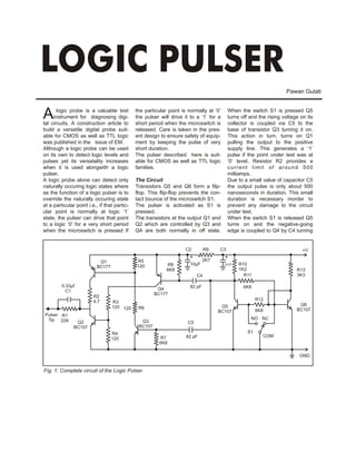
C2 R9 C3 +V
+ +
Q1 R5 2K7
120 R8 10µF 0.01 R10
BC177
6K8 1K2 R13
C4 R11 3K3
0.33µf 82 pF 6K8
C1 Q4
BC177
R2
4.7 R12
R3
Q5 Q6
120 120 R6
BC107 6K8 BC107
Pulser R1
Tip 22K NO NC
Q2 Q3 C5
BC107 BC107
R4 S1
R7 82 pF COM
120
6K8
GND.
Fig. 1: Complete circuit of the Logic Pulser.
2. EMDI003
Fig. 2: Actual size PCB Artwork
(View from Copper Side)
+
R9 300IDME
+V R5
R8 Q4
R13 R10 C2 Q1 C1
R11 R6 R2
R12 C3 R1
C4 R3
Q6 J C5 TIP OF PULSER
Q5 Q3 Q2
R7 R4
GND
N.C. N.O.
P
MICROSWITCH
Fig. 3: Component layout as shown from
Component side
it on. This turns on Q2 causing the current and the resistor R1 dis- 2 is employed. Fig. 3 shows the
output to be pulled to the negative charges C1 in between the pulses. component layout to be employed.
supply line. This gives a ‘0’ pulse The resistor R9 is for isolating the All the items except the microswitch
which is again of about 500 nano- high current pulse from the supply S1 can be assembled on the PCB.
seconds in duration. The R1,C1 capacitor C2 provides the actual Microswitches are available in many
combination at the pulser tip is to current. shapes and sizes. Try to get a min-
protect the pulser if it is accidently iature version which can be fitted in
connected to a point which is above Construction the pulser body.
or below the logic supply voltages. The construction of the pulser is A similar plastic case as used for the
While in use capacitor C1 carries the very simple if the PCB shown in Fig. logic probe can be employed to
Red Wire
PCB +
Assly.
Comp. Side Crockodile
Clips
Black Wire
GND.
18 SWG
Tinned Wire
About 1½” for TIP
NC
NO Microswitch
P S1
Fig. 4 : Complete Wiring diagram.
3. SPECIFICATIONS
! Supply voltage range = 5V to 15V D.C.
! Suitable for CMOS and TTL logic circuits
! Maximum supply current consumption = 15mA
! Drives capacitive loads upto 1000 pF
! Reverse polarity supply protection
! Output pulse duration = 500 nanoseconds
1
OR
SS F
PRE
FOR 0
ASE
EM RELE
ER
PU L S
Fig. 5 : Completed Pulser Fitted in A Plastic Enclosure
house the pulser.
COMPONENT LIST
Before wiring the
microswitch S1 check PART TOTAL Qty. DESCRIPTION
carefully its connec- R1 1 22K, ¼w ± 5% Resistor
tions with a multimeter.
R2 1 4.7Ohm, ½w ± 5% Resistor
One terminal wil be the
pole whereas the other R3, R4, R5, R6 4 120 Ohm, ¼w ± 5% Resistor
two are No and NC R7, R8,R12,R11 4 6K8, ¼w ± 5% Resistor
terminals. The NC
R9 1 2K7, ¼w ± 5% Resistor
terminal is the one
which is shorted to the R10 1 1K2, ¼w ± 5% Resistor
pole normally, and the R13 1 3K3, ¼w ± 5% Resistor
NO is the one which C1 1 0.33 µF Polyester
shorts to the pole when
the switch is kept C2 1 10 µF 25V Tantalum
pressed. C3 1 0.01 µF Polyester
You are advised to use C4,C5 2 82 pF Ceramic Disc
coloured wires for
Q2,Q3,Q5,Q6 4 BC 107 Transistor
switch connections
inorder to avoid wrong Q1,Q4 2 BC 177 Transistor
wiring. Keep the supply S1 1 Miniature Microswitch with one N.O. and One N.C. contacts
wires as short as possi-
MISC - Crockodile clips x2
ble, too long supply
wires can degrade the Flexible Hookup wire Red and Black 18 SWG Timed wire
performance of the about 1½” piece for Tip.
pulser.
Suitable plastic enclosure etc.