أسس الهندسة الإلكترونية
•
30 likes•5,347 views

مادة أسس الهندسة الالكترونية - سنة ثالثة - فصل أول- 2012 munthear@ gmail.com - الدكتور المهندس محمد منذر القادري

Recommended
Recommended
More Related Content
What's hot
What's hot (20)
Viewers also liked
Viewers also liked (20)
More from Dr. Munthear Alqaderi
More from Dr. Munthear Alqaderi (20)
Recently uploaded
Recently uploaded (20)
أسس الهندسة الإلكترونية
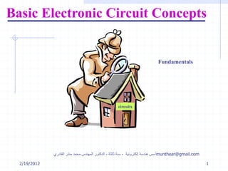
- 1. 2/19/2012 إلكترونية هندسة أسس-ثالثة سنة-القادري منذر محمد المهندس الدكتور munthear@gmail.com 1 Basic Electronic Circuit Concepts circuits Fundamentals
- 2. 2/19/2012 إلكترونية هندسة أسس-ثالثة سنة-الدكتور القادري منذر محمد المهندس munthear@gmail.com 2 Evolution of Electronics اإللكترونيات تطور 1941-1956 Vacuum Tube 1948 Transistor 1964-1971 Integrated circuit 1971 Microchip (VLSI) 1980 ULSI 1995 Nano Electronic
- 3. 2/19/2012 إلكترونية هندسة أسس-ثالثة سنة- القادري منذر محمد المهندس الدكتور munthear@gmail.com 3 الترانزستورالبكر المفرغ الصمام
- 4. 2/19/2012 إلكترونية هندسة أسس-ثالثة سنة-الدكتور القادري منذر محمد المهندس munthear@gmail.com 4
- 5. 2/19/2012 إلكترونية هندسة أسس-ثالثة سنة-الدكتور القادري منذر محمد المهندس munthear@gmail.com 5 Semiconductor Devices
- 6. 2/19/2012 إلكترونية هندسة أسس-ثالثة سنة-الدكتور القادري منذر محمد المهندس munthear@gmail.com 6
- 7. 2/19/2012 إلكترونية هندسة أسس-ثالثة سنة-الدكتور القادري منذر محمد المهندس munthear@gmail.com 7 اإللكترونية الهندسة أسس منهاج مفردات Semiconductor Devices Diodes Transistors BJT FET (MOFET, JFET) UJT Thyristors( SCR,SCS,PUT) Triac,Diac Optoelectronics
- 8. 2/19/2012 إلكترونية هندسة أسس-ثالثة سنة-الدكتور القادري منذر محمد المهندس munthear@gmail.com 8
- 9. SEMICONDUCTOR DEVICES 2/19/2012 إلكترونية هندسة أسس-ثالثة سنة-الدكتور القادري منذر محمد المهندس munthear@gmail.com 9
- 10. SEMICONDUCTOR DEVICES 2/19/2012 إلكترونية هندسة أسس-ثالثة سنة-الدكتور القادري منذر محمد المهندس munthear@gmail.com 10
- 11. SEMICONDUCTOR DEVICES 2/19/2012 إلكترونية هندسة أسس-ثالثة سنة-الدكتور القادري منذر محمد المهندس munthear@gmail.com 11
- 12. THE PROCESSOR 2/19/2012 إلكترونية هندسة أسس-ثالثة سنة-الدكتور القادري منذر محمد المهندس munthear@gmail.com 12
- 13. 2/19/2012 إلكترونية هندسة أسس-ثالثة سنة-الدكتور القادري منذر محمد المهندس munthear@gmail.com 13
- 14. 2/19/2012 إلكترونية هندسة أسس-ثالثة سنة-الدكتور القادري منذر محمد المهندس munthear@gmail.com 14 Direction of Current Flow
- 15. 2/19/2012 إلكترونية هندسة أسس-ثالثة سنة-الدكتور القادري منذر محمد المهندس munthear@gmail.com 15 النواقل أنصاف فيزيائية •موجبة شحنات ذات ونواة سالبة شحنات ذات الكترونات من الذرة تتألف •اإللكترون شحنة=1,6 exp –19 C •أكبر البروتون كتلة2000اإللكترون من مرة •البروتون كتلة=النيترون كتلة. •خاصة طاقة بمستويات النواة حول اإللكترونات تدور.ذات األقرب والمدارات أقل طاقة سويات. •ev=فولتا يساوي كمون فرق عبر إلكترون لتحريك الالزمة الطاقة كميةواحدا •الطاقة ثغرةenergy gapsإلكترون أية بها يوجد ال. •التكافؤ حزمةValence bandمهيجة غير لذرة األبعد الطاقة حزمة هي •نسبيا حرة اإللكترونات فيها تكون الناقلية حزمة.
- 16. 2/19/2012 إلكترونية هندسة أسس-ثالثة سنة-الدكتور القادري منذر محمد المهندس munthear@gmail.com 16 Resistance Charges passing through any conducting medium collide with the material at an extremely high rate and, thus, experience friction. The rate at which energy is lost depends on the wire thickness (area), length and physical parameters like density and temperature as reflected through the resistivity R l A
- 17. 2/19/2012 إلكترونية هندسة أسس-ثالثة سنة-الدكتور القادري منذر محمد المهندس munthear@gmail.com 17 Resistance Charges passing through any conducting medium collide with the material at an extremely high rate and, thus, experience friction. The rate at which energy is lost depends on the wire thickness (area), length and physical parameters like density and temperature as reflected through the resistivity R l A
- 18. 2/19/2012 إلكترونية هندسة أسس-ثالثة سنة-الدكتور القادري منذر محمد المهندس munthear@gmail.com 18 الطاقة حزم مخطط الناقلية حزمة التكافؤ حزمة الطاقة فجوة} إزدياد الطاقة
- 19. 2/19/2012 إلكترونية هندسة أسس-ثالثة سنة-الدكتور القادري منذر محمد المهندس munthear@gmail.com 19 والعوازل النواقل في التكافؤ حزم •أخرى إلى مادة من الطاقة حزم تختلف. •إلكت التستطيع حيث عريضة الطاقة ثغرة تكون العازلة المواد فيرونات بسهولة الناقلية حزمة إلى اإلنتقال التكافؤ. •الطاقة ثغرة تنعدم الناقلة المواد في EG=6ev EG=1ev التكافؤ حزمة التكافؤ حزمة التكافؤ حزمة الناقلية حزمة الناقلية حزمة الناقلية حزمة
- 20. 2/19/2012 إلكترونية هندسة أسس-ثالثة سنة-الدكتور القادري منذر محمد المهندس munthear@gmail.com 20 Intrinsic Semiconductor على السيلكون ذرة تحتوي14التكافؤ رباعي عنصر وهو إلكترون على الجرمانيوم ذرة تحتوي32التكافؤ رباعي عنصر وهو إلكترون
- 21. 2/19/2012 إلكترونية هندسة أسس-ثالثة سنة-الدكتور القادري منذر محمد المهندس munthear@gmail.com 21 Intrinsic Semiconductor . حر إلكترون ثقب -الذرية الروابط تنكسر للحرارة الناقل نصف بتعرض -شحنة كحامل يخدم الثقب
- 22. 2/19/2012 إلكترونية هندسة أسس-ثالثة سنة-الدكتور القادري منذر محمد المهندس munthear@gmail.com 22 النواقل وأنصاف النواقل في التيارالنقية
- 23. 2/19/2012 إلكترونية هندسة أسس-ثالثة سنة-الدكتور القادري منذر محمد المهندس munthear@gmail.com 23 Drift الجرف Applying an electric field across a semiconductor material, results in both types of carrier moving in opposite directions thus creating current flow.
- 24. 2/19/2012 إلكترونية هندسة أسس-ثالثة سنة-الدكتور القادري منذر محمد المهندس munthear@gmail.com 24 P-Type Semiconductor N-Type Semiconductor المعطية الشوائب:الفوسفور,األنتموان,الزرنيخ المستقبلة الشوائب:الجاليوم,األنديوم,البورون
- 25. 2/19/2012 إلكترونية هندسة أسس-ثالثة سنة-الدكتور القادري منذر محمد المهندس munthear@gmail.com 25 الفراغية البلورية البنية
- 26. 2/19/2012 إلكترونية هندسة أسس-ثالثة سنة-الدكتور القادري منذر محمد المهندس munthear@gmail.com 26 N-Type Semiconductor تشكل اإللكتروناتاألعظمية الحوامل والثقوباألقلية الحوامل بالزرني السليكون إشابةخ نوع ناقل نصف يعطيN
- 27. 2/19/2012 إلكترونية هندسة أسس-ثالثة سنة-الدكتور القادري منذر محمد المهندس munthear@gmail.com 27 P-Type Semiconductor تشكل الثقوباألعظمية الحوامل اإللكترونات واألقلية الحوامل بالجالي السليكون إشابةوم نوع ناقل نصف يعطيP
- 28. 2/19/2012 إلكترونية هندسة أسس-ثالثة سنة-الدكتور القادري منذر محمد المهندس munthear@gmail.com 28 Semiconductors Extrinsic semiconductors can be doped with both types of impurities, and their respective concentrations determine the type material they will become: N-type when ND > NA Majority carriers are free electrons and minority carriers are holes. P-type when ND < NA Majority carriers are holes and minority carriers are free electrons.
- 29. 2/19/2012 إلكترونية هندسة أسس-ثالثة سنة-الدكتور القادري منذر محمد المهندس munthear@gmail.com 29 Drift الجرف The magnitude of the electric field in volts/cm is given by: And the effective velocity of the carrier moving by the drift action of an applied electric filed is given by: Where n = 1350 cm2/V-s and p = 480 cm2/V-s are the electron and hole mobility constants respectively. L V E Ennv Eppv
- 30. 2/19/2012 إلكترونية هندسة أسس-ثالثة سنة-الدكتور القادري منذر محمد المهندس munthear@gmail.com 30 P-N Junction Created by bringing together a p-type and n-type region within the same semiconductor lattice.
- 31. 2/19/2012 إلكترونية هندسة أسس-ثالثة سنة-الدكتور القادري منذر محمد المهندس munthear@gmail.com 31 The Diode n p p n B A SiO2 Al A B Al A B Cross-section of pn-junction in an IC process One-dimensional representation diode symbol
- 32. 2/19/2012 إلكترونية هندسة أسس-ثالثة سنة-الدكتور القادري منذر محمد المهندس munthear@gmail.com 32 At the junction, free electrons from the N-type material fill holes from the P-type material. This creates an insulating layer in the middle of the diode called the depletion zone. الوصلة نظريةP-N
- 33. 2/19/2012 إلكترونية هندسة أسس-ثالثة سنة-الدكتور القادري منذر محمد المهندس munthear@gmail.com 33 E
- 34. 2/19/2012 إلكترونية هندسة أسس-ثالثة سنة-الدكتور القادري منذر محمد المهندس munthear@gmail.com 34 المحرمة المنطقة عرض - --- - ---- - ---- - ----- + + + + + + + + + + + + + + + + - - - - - - - - + + + + + + + + اإلشابة مستوى على يعتمد المحرمة المنطقة عرض إن P PN N 1 micron Depletion
- 35. 2/19/2012 إلكترونية هندسة أسس-ثالثة سنة-الدكتور القادري منذر محمد المهندس munthear@gmail.com 35
- 36. 2/19/2012 إلكترونية هندسة أسس-ثالثة سنة-الدكتور القادري منذر محمد المهندس munthear@gmail.com 36 Depletion Region الناضبة المنطقة hole diffusion electron diffusion p n hole drift electron drift Charge Density Distance x+ - Electrical xField x Potential V W2-W1 (a) Current flow. (b) Charge density. (c) Electric field. (d) Electrostatic potential.
- 37. 2/19/2012 إلكترونية هندسة أسس-ثالثة سنة-الدكتور القادري منذر محمد المهندس munthear@gmail.com 37 E E
- 38. 2/19/2012 إلكترونية هندسة أسس-ثالثة سنة-الدكتور القادري منذر محمد المهندس munthear@gmail.com 38
- 39. 2/19/2012 إلكترونية هندسة أسس-ثالثة سنة-الدكتور القادري منذر محمد المهندس munthear@gmail.com 39 Conductivity أنصاف في الناقلية النواقل Property of a material. It is a measure of the material’s ability to to carry electric current. It is given in Semiconductor by: Measured in S-cm. pn pnq
- 40. 2/19/2012 إلكترونية هندسة أسس-ثالثة سنة-الدكتور القادري منذر محمد المهندس munthear@gmail.com 40 Why Semiconductors?
- 41. 2/19/2012 إلكترونية هندسة أسس-ثالثة سنة-الدكتور القادري منذر محمد المهندس munthear@gmail.com 41 Forward Bias األمامي اإلنحياز x pn0 np0 -W1 W2 0 pn(W2) n-regionp-region Lp diffusion
- 42. 2/19/2012 إلكترونية هندسة أسس-ثالثة سنة-الدكتور القادري منذر محمد المهندس munthear@gmail.com 42 Reverse Bias العكسي اإلنحياز x pn0 np0 -W1 W20 n-regionp-region diffusion
- 43. 2/19/2012 إلكترونية هندسة أسس-ثالثة سنة-الدكتور القادري منذر محمد المهندس munthear@gmail.com 43 Potential Barrier الكموني الحاجز The charge barrier creates a state of balance with the diffusion process, and this barrier can be represented as a voltage or potential barrier.
- 44. 2/19/2012 إلكترونية هندسة أسس-ثالثة سنة-الدكتور القادري منذر محمد المهندس munthear@gmail.com 44 Resistivity المقاومية Measured in -cm it is the reciprocal of conductivity: The resistance of a material with constant cross section can be calculated by: 1 A L R ne المعادن في الناقلية االلكترونات حركيةn الحرة االلكترونات تركيز e االلكترون شحنة
- 45. 2/19/2012 إلكترونية هندسة أسس-ثالثة سنة-الدكتور القادري منذر محمد المهندس munthear@gmail.com 45 التيار كثافةCurrent Density Current per unit cross-sectional area. Measured in A/cm2. Given by: n الحرة اإللكترونات تركيز , p الثقوب تركيز الثقوب تركيز * The direction of current flow vector is the same direction as the electric field vector. qEp p )(nEJ n
- 46. 2/19/2012 إلكترونية هندسة أسس-ثالثة سنة-الدكتور القادري منذر محمد المهندس munthear@gmail.com 46 Diffusion اإلنتشار Diffusion current occurs because of the physical principle that over time particles undergoing random motion will show a movement from a region of high concentration to a region of lower concentration.
- 47. 2/19/2012 إلكترونية هندسة أسس-ثالثة سنة-الدكتور القادري منذر محمد المهندس munthear@gmail.com 47 Diffusion Current density is directly proportional to the gradient of carrier concentration. Dn and Dp are the diffusion constants for electrons and holes respectively. dx dn qDJ nn dx dp qDJ pp
- 48. 2/19/2012 إلكترونية هندسة أسس-ثالثة سنة-الدكتور القادري منذر محمد المهندس munthear@gmail.com 48 Diffusion Capacitance
- 49. 2/19/2012 إلكترونية هندسة أسس-ثالثة سنة-الدكتور القادري منذر محمد المهندس munthear@gmail.com 49
- 50. 2/19/2012 إلكترونية هندسة أسس-ثالثة سنة-الدكتور القادري منذر محمد المهندس munthear@gmail.com 50 Diodes الناقل نصف الوصلة ثنائي A diode can be considered to be an electrical one-way valve. They are made from a large variety of materials including silicon, germanium, gallium arsenide, silicon carbide … ANODE D1 DIODE CATHODE
- 51. 2/19/2012 إلكترونية هندسة أسس-ثالثة سنة-الدكتور القادري منذر محمد المهندس munthear@gmail.com 51
- 52. 2/19/2012 إلكترونية هندسة أسس-ثالثة سنة-الدكتور القادري منذر محمد المهندس munthear@gmail.com 52 المثالي الناقل نصف الثنائي
- 53. 2/19/2012 إلكترونية هندسة أسس-ثالثة سنة-الدكتور القادري منذر محمد المهندس munthear@gmail.com 53 Diode Current
- 54. 2/19/2012 إلكترونية هندسة أسس-ثالثة سنة-الدكتور القادري منذر محمد المهندس munthear@gmail.com 54 Diode V-I Characteristic For ideal diode, current flows only one way Real diode is close to ideal Ideal Diode
- 55. 2/19/2012 إلكترونية هندسة أسس-ثالثة سنة-الدكتور القادري منذر محمد المهندس munthear@gmail.com 55 Piecewise Linear Model The real diode can be approximated by a model which uses two connected line segments. Note that the turn on voltage, VF , marks the point where the two line segments meet.
- 56. 2/19/2012 إلكترونية هندسة أسس-ثالثة سنة-الدكتور القادري منذر محمد المهندس munthear@gmail.com 56 The Diode Equation The diode equation can be derived based on the assumption that carriers move by diffusion. ID – Current through diode. IO – Reverse saturation current. VD – Voltage across the diode. k – Boltzmann’s Constant. n – Ideality factor (n = 1 for silicon). T – Temperature in degrees Kelvin. 1nkT qV OD D eII 39 kT q
- 57. 2/19/2012 إلكترونية هندسة أسس-ثالثة سنة-الدكتور القادري منذر محمد المهندس munthear@gmail.com 57 Dp/µp=DN /µN=VT الحرارة لدرجة المكافئ الفولت(انشتاين عالقة) VT=KT/e=T/11600 at 300K
- 58. 2/19/2012 إلكترونية هندسة أسس-ثالثة سنة-الدكتور القادري منذر محمد المهندس munthear@gmail.com 58 للثنائي الحرارية الخواص V(T1)-V(T0)=KT(T1-T0) KT=-2.5mv/c Ge KT==2.0mv/c Si I0(T2)=I0(T1)exp[Ki(T2-T1)] Ki=0.07/C
- 59. 2/19/2012 إلكترونية هندسة أسس-ثالثة سنة-الدكتور القادري منذر محمد المهندس munthear@gmail.com 59 الناقل نصف الثنائي مقاومة 1nkT qV OD D eII T o T v v o V II V eI dv dI g T الديناميكية الناقلية الديناميك المقاومة تكون وبالتالي جدا صغيرة الناقلية تكون العكسي اإلنحياز حالة فيجدا كبيرة ية يكون األمامي اإلنحياز حالة فيIo<<Iيكون وبالتالي: I V g r T 1 I mv I V r T 26
- 60. 2/19/2012 إلكترونية هندسة أسس-ثالثة سنة-الدكتور القادري منذر محمد المهندس munthear@gmail.com 60 The Diode Model 0.7V Rr Rf Rr Cf CD Cf rd الم للتيار المكافئة الدارةستمر األم اإلنحياز في المتناوب للتيار المكافئة الدارةامي اإلنحياز في المتناوب للتيار المكافئة الدارةالعكسي
- 61. 2/19/2012 إلكترونية هندسة أسس-ثالثة سنة-الدكتور القادري منذر محمد المهندس munthear@gmail.com 61 الحمل خط مفهومLoad Line Vo Io Vs r R Io Vs Vo Io Vo=R . Io Vo=Vs - IoRs o Q point
- 62. 2/19/2012 إلكترونية هندسة أسس-ثالثة سنة-الدكتور القادري منذر محمد المهندس munthear@gmail.com 62 الديناميكي الحمل خطAC- Load Line Vs+vs R1 R2 C iD vD -1/Rdc -1/Rac Q
- 63. 2/19/2012 إلكترونية هندسة أسس-ثالثة سنة-الدكتور القادري منذر محمد المهندس munthear@gmail.com 63 Graphical Solution Simplify the circuit connected to the diode to a Thevenin’s equivalent circuit. Analyze two cases: iD = 0; vD = 0. This two points identifies the Thevenin’s circuit load line, and this lines intersects the diode plot at the operating point. البياني الحل
- 64. 2/19/2012 إلكترونية هندسة أسس-ثالثة سنة-الدكتور القادري منذر محمد المهندس munthear@gmail.com 64 مثالي لثنائي التقويم مبدأ
- 65. 2/19/2012 إلكترونية هندسة أسس-ثالثة سنة-الدكتور القادري منذر محمد المهندس munthear@gmail.com 65 المتناوب التيار تقويم مبدأ الدو التابع متوسط هو الناتج المستمر الجهدري
- 66. 2/19/2012 إلكترونية هندسة أسس-ثالثة سنة-الدكتور القادري منذر محمد المهندس munthear@gmail.com 66 المقومة الموجة تنعيم Vs=V
- 67. 2/19/2012 إلكترونية هندسة أسس-ثالثة سنة-الدكتور القادري منذر محمد المهندس munthear@gmail.com 67 Full-wave Rectification The output of a full- wave rectifier is driven by both the positive and negative cycles of the sinusoidal input, unlike the half-wave rectifier which uses only one cycle.
- 68. 2/19/2012 إلكترونية هندسة أسس-ثالثة سنة-الدكتور القادري منذر محمد المهندس munthear@gmail.com 68 Diode Bridge
- 69. 2/19/2012 إلكترونية هندسة أسس-ثالثة سنة-الدكتور القادري منذر محمد المهندس munthear@gmail.com 69 التعرج حساباتRipple Full-wave ripple frequency is twice AC frequency Ripple Factor=Vr(rms)/Vdc
- 70. 2/19/2012 إلكترونية هندسة أسس-ثالثة سنة-الدكتور القادري منذر محمد المهندس munthear@gmail.com 70 Filtering The reduction in voltage between charging cycles is dependent on the time constant stated below: t m L eVtv CR
- 71. 2/19/2012 إلكترونية هندسة أسس-ثالثة سنة-الدكتور القادري منذر محمد المهندس munthear@gmail.com 71 Ripple Factor Ripple is the small voltage variation from the filter’s output. Good power supplies produce as little ripple as possible. Ripple is usually specified as Ripple Factor, RF : valuedc rippleofvaluerms RF
- 72. 2/19/2012 إلكترونية هندسة أسس-ثالثة سنة-الدكتور القادري منذر محمد المهندس munthear@gmail.com 72 Voltage Doubler
- 73. 2/19/2012 إلكترونية هندسة أسس-ثالثة سنة-الدكتور القادري منذر محمد المهندس munthear@gmail.com 73 Voltage Doubler Voltage doublers allow you to develop higher voltages without a transformer. Stages can be cascaded to produce triplers, quadruplers, etc. Voltage multipliers usually supply low currents to a high-resistance load. Output voltage usually drops quickly as load current increases.
- 74. 2/19/2012 إلكترونية هندسة أسس-ثالثة سنة-الدكتور القادري منذر محمد المهندس munthear@gmail.com 74 الموجات تشكيل
- 75. 2/19/2012 إلكترونية هندسة أسس-ثالثة سنة-الدكتور القادري منذر محمد المهندس munthear@gmail.com 75 Diode Types Rectifier Diode Fast Recovery Diode Zener Diode Current Regulator Diode Schottky Diode Varactor Diodes Tunnel Diode PIN Diode Photodiode Light Emitting Diode (LED) Laser Diode
- 76. 2/19/2012 إلكترونية هندسة أسس-ثالثة سنة-الدكتور القادري منذر محمد المهندس munthear@gmail.com 76 Diode Applications Rectifying Reverse Voltage Protection Over voltage protection Switching Signal shaping Variable Capacitor Variable Resistor Oscillator Display Light Sensing Temperature Sensing
- 77. 2/19/2012 إلكترونية هندسة أسس-ثالثة سنة-الدكتور القادري منذر محمد المهندس munthear@gmail.com 77
- 78. 2/19/2012 إلكترونية هندسة أسس-ثالثة سنة-الدكتور القادري منذر محمد المهندس munthear@gmail.com 78
- 79. 2/19/2012 إلكترونية هندسة أسس-ثالثة سنة-الدكتور القادري منذر محمد المهندس munthear@gmail.com 79 Zener Diode
- 80. 2/19/2012 إلكترونية هندسة أسس-ثالثة سنة-الدكتور القادري منذر محمد المهندس munthear@gmail.com 80
- 81. 2/19/2012 إلكترونية هندسة أسس-ثالثة سنة-الدكتور القادري منذر محمد المهندس munthear@gmail.com 81
- 82. 2/19/2012 إلكترونية هندسة أسس-ثالثة سنة-الدكتور القادري منذر محمد المهندس munthear@gmail.com 82 Diodes - Simple Applications Why would you want the equivalent of an electronic check- valve?
- 83. 2/19/2012 إلكترونية هندسة أسس-ثالثة سنة-الدكتور القادري منذر محمد المهندس munthear@gmail.com 83 Diode Current-Voltage relationship The characteristics of all silicon based diodes are effectively the same, showing a sharp exponential increase in current at forward bias and only a few As at reverse bias. Note that this “knee” is temperature- dependent as observed in lab 1. The non-ideal behavior shows a slower than exponential increase due to a series resistance, like the inductor. At large reverse-bias (not shown) current starts to flow. We will discuss this region later. 1N4148 characteristics
- 84. 2/19/2012 إلكترونية هندسة أسس-ثالثة سنة-الدكتور القادري منذر محمد المهندس munthear@gmail.com 84 Diode models A diode is often approximated as a 2-terminal device with ~0.7 v drop as long as 1-100 mA are flowing in the forward direction. The curves for a typical switching signal diode show why this is OK (note the log scale for current). When it is either reverse or weakly forward biased it is modeled as an open circuit. Real diodes and the symbol are shown. The arrow points in the direction of forward current flow.
- 85. 2/19/2012 إلكترونية هندسة أسس-ثالثة سنة-الدكتور القادري منذر محمد المهندس munthear@gmail.com 85 More Diode Physics Pure semiconducting materials like Silicon have very high resistivity at room temperature. However it can be made conductive by adding extra electrons. In n-type material this is done via atoms with one more electron than silicon (phosphorus). It can also be more conductive if one electron is removed, allowing the resulting “holes” to move about (they are really absences of valence or bonding electrons that hop from one site to the next). This is done in p-type material by adding elements with one less electron (aluminum). This is known as doping. An interesting thing happens if p- and n-type material are in contact. A region that has no holes on the p-side and no electrons on the n-side forms, called the depletion region. This area is like the original pure semiconductor and does not conduct, making the junction a very poor conductor again. However if it is biased (meaning a voltage is applied) with the p-type positive relative to the n- type, the depletion region shrinks. This is the origin of the one-way flow. The next slides describe why this is, using images from the website http://jas.eng.buffalo.edu/
- 86. 2/19/2012 إلكترونية هندسة أسس-ثالثة سنة-الدكتور القادري منذر محمد المهندس munthear@gmail.com 86 When material with lots of electrons (n-type) is brought into contact with material with lots of holes (p-type) the electrons and holes diffuse, resulting in a large current. However the loss of these carriers leaves a depleted region that is charged (because of the P and Al ions left behind) and reduces the current since the electric field repels the carriers. Diode Current-Voltage relationship (1)
- 87. 2/19/2012 إلكترونية هندسة أسس-ثالثة سنة-الدكتور القادري منذر محمد المهندس munthear@gmail.com 87 Diode Current-Voltage relationship (2) At zero bias electrons (holes) flow left (right) because of diffusion and an equal amount flow right (left) due to the electric field, resulting in no current. As the depletion region increases with reverse bias (not shown), the diffusion current to the left decreases leaving only a small reverse saturation current due to the field. Notice that for these doping levels the depletion region is 0.15 microns thick.
- 88. 2/19/2012 إلكترونية هندسة أسس-ثالثة سنة-الدكتور القادري منذر محمد المهندس munthear@gmail.com 88 Diode Current-Voltage relationship (3) At positive bias the depletion region is reduced and many electrons (holes) diffuse left (right) while only a small amount flow right (left) due to the electric field, resulting in a large current (sum of holes and electrons) flowing right. When an electron gets to the p- type material it recombines with a hole. If it does this in the depleted region the ideality factor N is 2, while it is 1 if recombination occurs outside. The depletion region is now only 0.05 microns thick.
- 89. 2/19/2012 إلكترونية هندسة أسس-ثالثة سنة-الدكتور القادري منذر محمد المهندس munthear@gmail.com 89 Types of diodes Power diodes (or rectifiers) - designed to handle large currents, typically used on power supplies or for switches. Typical values (for 1N4002) Max Average current: 1 A Peak current: 30 A Reverse voltage: 100 v Signal diodes - low powered, often faster switching (smaller depletion region). Typical values (for 1N4148) Max Average current: 100 mA Peak current: 450 mA Reverse voltage: 75 v Recovery time: 4 ns Zener diodes - voltage regulation, similar to power diodes but has any important specification: the zener voltage, Vz (more later). Designed to breakdown at precise voltage (range 1-400 v).
- 90. 2/19/2012 إلكترونية هندسة أسس-ثالثة سنة-الدكتور القادري منذر محمد المهندس munthear@gmail.com 90 Clamp (or clipper) Vin R Vout What does this circuit do? As mentioned in the text it “clamps” or “clips” the output voltage. If the magnitude of the input exceeds Vbatt+0.7 v, either negative or positive, the diode starts conducting. This limits the maximum voltage (this is similar to surge protectors). Vbat One limitation of this is that by design it will distort a time- varying voltage input, cutting it off at a max and a min value.
- 91. 2/19/2012 إلكترونية هندسة أسس-ثالثة سنة-الدكتور القادري منذر محمد المهندس munthear@gmail.com 91 Stiff Clamp Vin C Vout This circuit on the other hand works very well at higher frequencies in limiting the minimum voltage on the output. Treating the diode like a simple one-way switch we see that the output can never fall below -0.7 v, because then the diode begins conducting. How does the circuit do this? If the input voltage is less than this minimum, current flows counterclockwise, charging the left capacitor plate negative and the right plate positive. This capacitor voltage adds to the input, raising it to a minimum of -0.7 v, when current stops flowing. Note that it is the opposite if the diode is reversed because the currents flow clockwise.
- 92. 2/19/2012 إلكترونية هندسة أسس-ثالثة سنة-الدكتور القادري منذر محمد المهندس munthear@gmail.com 92 Zener diode - IV characteristics All diodes show a breakdown under reverse bias when the internal electric field gets very high, ripping electrons from atoms. This avalanche breakdown occurs typically at -50 to -1000 v. If the depleted region that acts like a barrier to current is thin there is another possibility. The electrons can quantum mechanically tunnel from the n- to the p- side, resulting in a reverse current. This can be engineered to occur at a precise voltage called the Zener voltage, VZ. V I VZ IIIIII The graph shows three distinct regions, as labeled. Region III is where zener diodes normally operate.
- 93. 2/19/2012 إلكترونية هندسة أسس-ثالثة سنة-الدكتور القادري منذر محمد المهندس munthear@gmail.com 93 Zener diode - voltage regulator (1) How can a zener regulator act to control the output voltage? In the circuit shown (note that the zener is connected so that it is reverse biased) current flows through the zener and it is in region III, so the voltage drop across it is VZ. A zener only works as a regulator because it ensures that enough current is drawn through the series resistor so that the voltage drop results in Vout=VZ. If no current flows through the zener (actually less than a few mAs) it no longer regulates because it is in region II. Vout UnregulatedVin
- 94. 2/19/2012 إلكترونية هندسة أسس-ثالثة سنة-الدكتور القادري منذر محمد المهندس munthear@gmail.com 94 Zener diode - voltage regulator (2) Rload UnregulatedVin Rload UnregulatedVin The voltage across the load is VZ since there is current through the zener (Region III) RR The voltage on the load is Rload/(R+Rload)Vin because there is no current through the zener.