
Recommended
Recommended
More Related Content
What's hot
What's hot (20)
Viewers also liked
Viewers also liked (16)
Similar to Logic gate class 12
Similar to Logic gate class 12 (20)
Recently uploaded
Recently uploaded (20)
Logic gate class 12
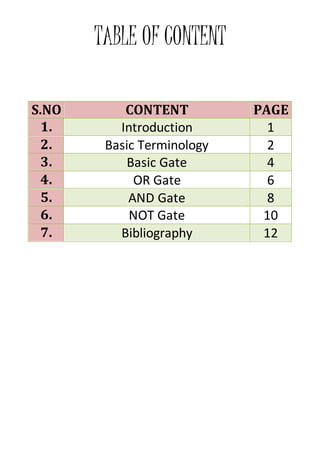
- 1. TABLE OF CONTENT S.NO CONTENT PAGE 1. Introduction 1 2. Basic Terminology 2 3. Basic Gate 4 4. OR Gate 6 5. AND Gate 8 6. NOT Gate 10 7. Bibliography 12
- 2. INTRODUCTION A logic gate can be defined as digital circuit which either allows a signal to pass through or stops it. These gates are related to Boolean Algebra . These gates allow signals to pass through them only when some logic is satisfied. A semiconductor diode (P‐N junction) acts as a closed switch when it is forward biased, i.e. it allows current to pass through it. It acts as an open circuit when it is reversed biased, i.e. it allows very little or no current to pass through it. This unique property of diode is employed in the design of logic gates and the circuits. The logic gates are building blocks of electronic devices. Logic gate may have one or more inputs but can only have one output. Possible values of input and output of logic gates are expressed in form of tables called truth tables. Two values of logic statement are denoted by binary numbers 1 and 0 where 1 represent higher value. 1.
- 3. BASIC TERMINOLOGY SIGNAL :- Information converted in electrical form and suitable for transmissionis called a signal. There are two types of signals:‐ i) Analog signal ii)Digital signal ANALOG SIGNAL :- Analog signals are continuous variation of voltage or current. They are essentially single‐valued function of time. Sine wave is fundamental analog signal DIGITAL SIGNAL :- Digital signal are those which can take only discrete step wise values. Binary system that is extensively used in digital electronics employs just two levels of a signal. ‘O’ corresponds to low level and ‘1’ corresponds to high level of voltage or current. 2.
- 4. LOGICGATE :- A digital circuit which allows a signal to pass through it or stops is called a gate. When such gate allows the signal to pass through only when some logical condition is satisfied, they are called logic gates. Each logic gate follows certain logical relationship between input and output voltage. It is used in calculators, etc. DIGITAL CIRCUIT :- The electrical circuit which uses only digital signals is called digital circuit. 3.
- 5. BASIC GATES There are three basic logic gates. They are combined together to form several other logic gate. These logic gates are the building block of digital circuit. The basic logic gates are:‐ 1. OR GATE 2. AND GATE 3.NOT GATE The logic gates are represented with specific symbols in digital circuit. 1. OR GATE Boolian expression = A+B =Y Where A and B are input while Y is output and (+) indicates OR. 4.
- 6. 2. AND GATE Boolian expression = A.B =Y Where A and B are input while Y is output and (.) indicates AND. 3. NOT GATE Boolian expression = Ã =Y Where A and B are input while Y is output and (~) indicates NOT. 5.
- 7. OR GATE AIM To simulate and design the OR Gate COMPONENTS Two ideal p-n junction diodes (D1 and D2) THEORY AND CONSTRUCTION An OR Gate can be idealized by using two identical diode as shown in figure.Here negative terminal of battery is grounded and corresponded to 0 level and positive terminal correspond to 1 level. TRUTH TABLE INPUT A INPUT B OUTPUT Y 1 0 1 1 1 1 0 1 1 0 0 0
- 8. 6. . INTERFERENCE a) IF A and B are open LED do not glow {A=0 B=0} so A+B=Y , hence Y=0. b) IF A and B are closed LED will glow {A=1 B=1} so A+B=Y , hence Y=1. c) IF A is open and B is closed LED will glow {A=0 B=1} so A+B=Y , hence Y=1. d) IF A is closed and B is open LED will glow {A=1 B=0} so A+B=Y , hence Y=1. 7.
- 9. AND GATE AIM To simulate and design the AND Gate COMPONENTS Two n-p-n transistors and Resistance R and R2 THEORY AND CONSTRUCTION An OR Gate can be idealized by using two identical diode as shown in figure. Resistance R2 is earthed while R is connected to both ends of Battery. Here negative terminal of battery is grounded and corresponded to 0 level and positive terminal correspond to 1 level. TRUTH TABLE INPUT A INPUT B OUTPUT Y 1 0 0 1 1 1 0 1 0
- 10. 0 0 0 8. . INTERFERENCE a) IF A and B are open LED do not glow {A=0 B=0} so A.B=Y , hence Y=0. b) IF A and B are closed LED will glow {A=1 B=1} so A.B=Y , hence Y=1. c) IF A is open and B is closed LED will glow {A=0 B=1} so A.B=Y , hence Y=0. d) IF A is closed and B is open LED will glow {A=1 B=0}
- 11. so A.B=Y , hence Y=0. 9. NOT GATE AIM To simulate and design the NOT Gate COMPONENTS n-p-n transistor THEORY AND CONSTRUCTION NOT Gate cannot be realized by using diodes but can be done by using n-p-n transistor. Base b is connected to input A while Emitter is earthed and collector is connected to battery. TRUTH TABLE INPUT A OUTPUT Y
- 12. 1 0 0 1 10. . INTERFERENCE a) IF A is closed LED do not glow {A=1} so à =Y , hence Y=0. b) IF A is open LED will glow {A=0} so à =Y , hence Y=1.
- 13. 11. BIBLIOGRAPHY 1. www.wikipedia.com 2. www.google.com 3. www.answers.com 4. NCERT Vol. 1 and 2 Physics Class 12 5. Pradeep Class 12 Physics 6. HC Verma Physics Part 2