Lesson4
•Download as PPT, PDF•
1 like•1,186 views

Resonant Circuits as Filters,Transformers,A Simple Amplifier,Common Collector Amplifier,The SW+ Driver

Recommended
More Related Content
What's hot
What's hot (20)
Similar to Lesson4
Similar to Lesson4 (20)
More from Kavin Paul
Recently uploaded
Recently uploaded (20)
Lesson4
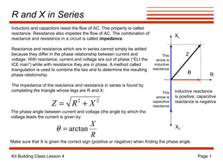
- 1. R and X in Series Inductors and capacitors resist the flow of AC. This property is called reactance. Resistance also impedes the flow of AC. The combination of reactance and resistance in a circuit is called impedance . Reactance and resistance which are in series cannot simply be added because they differ in the phase relationship between current and voltage. With reactance, current and voltage are out of phase (“ELI the ICE man”) while with resistance they are in phase. A method called triangulation is used to combine the two and to determine the resulting phase relationship. The impedance of the reactance and resistance in series is found by completing the triangle whose legs are R and X: X L X C R Z The phase angle between current and voltage (the angle by which the voltage leads the current is given by: This arrow is inductive reactance This arrow is capacitive reactance inductive reactance is positive; capacitive reactance is negative Make sure that X is given the correct sign (positive or negative) when finding the phase angle.
- 2. R and X in Parallel For a parallel combination of resistance and reactance, we use a different formula for finding the resulting impedance: In this case, the phase angle by which voltage leads current is given by If the reactance is capacitive, the phase angle is negative. If the reactance is inductive, the phase angle is positive. Ohm’s Law for Impedance
- 3. Resonant Circuits as Filters A series resonant circuit has a very low impedance at the resonant frequency and a high impedance at other frequencies. It acts as a bandpass filter by passing the resonant frequency but impeding others. A parallel-resonant circuit presents a high impedance to the resonant frequency and low impedance to other frequencies. It provides a path to ground for the nonresonant frequencies. Real circuits like this have resistance as well as inductance and capacitance. The resistance plays a role in determining the bandwidth of the filter. The Q of the circuit is an indication of the bandwidth of the filter (X is the reactance of either the inductoror the capacitor): The bandwidth of the filter (range of frequencies where the current is greater than 0.707 of its maximum value) is:
- 4. Transformers Transformers are devices which use magnetic fields as a means of transforming (changing) voltage, current, or impedance. They are used with AC signals. When current is made to flow in the primary winding of the transformer, it creates a magnetic field. As the current in the primary changes (it’s an AC signal, remember) the magnetic field changes. The secondary winding sees the changing magnetic field, and this causes current to flow in it. AC Load primary secondary The amount of voltage, current, and impedance in the secondary is determined by that in the primary and the ratio of turns in the secondary to the primary:
- 5. Bandpass Filter in the SW+ The SW+ uses two 10.7 MHz IF transformers back to back as a bandpass filter. These transformers have built-in capacitors to act as tuned circuits. The SW+ adds capacitors in parallel with the primaries to lower the resonant frequency of the transformer primaries. Capacitor C31 acts with the secondary windings to form a series LC circuit, so there are three separate tuned circuits in the bandpass filter. circuit copyright 1998 Dave Benson NN1G
- 6. Transistor AC Amplification +E R C R B Remember that changes in the base current in a transistor cause the collector current to change. If the base current changes due to an applied AC signal, the collector current will change in the same way. As the collector current changes, the voltage drop across resistor R C changes, causing the collector voltage to change as well. V C V B V C I C E E/R C 0 0 saturation linear region cutoff In order to obtain a faithfully amplified copy of the input signal, the transistor must be biased so that it operates in its linear region. The transistor should be biased so that the collector voltage never enters the saturation region or cutoff region. In those regions, the gain is not linear, and distortion of the signal results.
- 7. A Simple Amplifier +E R C R B V C V B How do we bias this transistor so that the collector voltage will be about half of the supply voltage E? Let’s assume that E is 12 volts and we want a collector current of 10 mA. That means the voltage drop across R C needs to be 6V. If 10 mA flows through R C we can find the value of R C : Next, we need to find the value of the bias resistor R B so that the base current is at the appropriate level. Base current needs to be (assuming of 100) 100 A so that the collector current is 10 mA. So, R B can be found by: The voltage gain A V of this amplifier is the ratio of change in output voltage to change in input voltage and is given by: What happens if changes (say because of a change in temperature? Then collector current changes, the voltage across R C changes, and the DC bias of V C changes. R in is the input impedance of the transistor. R L is the load on the output (here, R C ). note the inverted output!
- 8. Common Emitter Amplifier +E R C R 1 V C V B R E R 2 The simple amplifier we just reviewed suffers from instability due to sensitivity to and R in with temperature. A better design is the common emitter circuit, shown here. R 1 and R 2 form a voltage divider which effectively sets the DC voltage at the base. The voltage at the emitter must be equal to the base voltage minus 0.6V, and all this voltage must be dropped across R E . This determines how much current must flow through R E and thus through R C . That sets the DC bias of the collector. Note how the base and collector currents were figured out without concern for the of the transistor. This design is much more temperature-stable than the simpler design. For the common emitter circuit, the voltage gain is given by This circuit sacrifices high gains for stability. Adding a capacitor in parallel with R E restores some of the of the gain by making the emitter appear grounded to AC signals, much like the previous design.
- 9. Common Collector Amplifier +E R 1 V E V B R E R 2 The common collector circuit (also known as the emitter follower ) changes the common emitter by deleting the collector resistor and taking the output from the emitter. The common collector circuit exhibits current gain but no voltage gain. Since the emitter voltage is always less than the base voltage, the voltage gain is essentially one. Why use a common collector amplifier? Because of its input and output impedances. The common collector input is high-impedance, while its output is low impedance. The high input impedance means that it draws very little current from the signal source. This means that the signal source is not affected very much by the common collector circuit. The low output impedance means that it has the ability to supply current to the load with no problem. Because of its input and output characteristics, it can serve as a buffer between successive stages of a circuit, preventing them from influencing each other. output not inverted!
- 10. The SW+ Transmit Buffer Q4 is the transistor used in the SW+ buffer circuit. The buffer keeps the rest of the transmit chain from affecting the output from the mixer. The voltage divider made by R22 and R23 biases the base to about 4V. The emitter resistor R24 is actually a trimmer pot. It is used to adjust the current being fed to the base of Q5. The output of the buffer is taken from the emitter, making this a common collector amplifier. circuit copyright 1998 Dave Benson NN1G
- 11. The SW+ Driver The SW+ driver is a common emitter circuit whose job is to provide some of the gain of the transmitter. Its output is taken from the collector and fed to the base of the power transistor Q6 via a transformer for impedance matching. R25 and R26 provide the DC bias for the base. Note the use of two resistors in series at the collector, with a capacitor in parallel with one. This scheme is a compromise between gain and stability. circuit copyright 1998 Dave Benson NN1G