SlideShare a Scribd company logo
1 of 6
Download to read offline
Power Electronics Technology June 2006 www.powerelectronics.comJune 2006 www.powerelectronics.com46
Buck-Converter
Design Demystified
Though stepdown converters are extremely
popular,therulesofthumbandcalculationsthat
speed their design can be hard to find.
By Donald Schelle and Jorge Castorena,Technical Staff,Jorge Castorena,Technical Staff,Jorge Castorena,
Maxim Integrated Products,Sunnyvale,Calif.
S
tepdown (buck) switching converters are integral
to modern electronics.They can convert a voltage
source (typically 8 V to 25 V) into a lower regu-
lated voltage (typically 0.5 V to 5 V). Stepdown
converters transfer small packets of energy using a
switch, a diode, an inductor and several capacitors. Though
substantially larger and noisier than their linear-regulator
counterparts, buck converters offer higher efficiency in
most cases.
Despite their widespread use, buck-converter designs
can pose challenges to both novice and intermediate power-
supply designers because almost all of the rules of thumb
and some of the calculations governing their design are
hard to find. And though some of the calculations are read-
ily available in IC data sheets, even these calculations are
occasionally reprinted with errors. In this article, all of the
design information required to design a buck converter is
conveniently collected in one place.
Buck-converter manufacturers often specify a typical
application circuit to help engineers quickly design a working
prototype, which in turn often specifies component values
and part numbers. What they rarely provide is a detailed
description of how the components are selected. Suppose
a customer uses the exact circuit provided. When a critical
component becomes obsolete or a cheaper substitute is
needed,the customer is usually without a method for select-
ing an equivalent component.
This article covers only one stepdown regulator topology
one with a fixed switching frequency, pulse width modu-one with a fixed switching frequency, pulse width modu-
lation (PWM) and operation in the continuous-current
mode (CCM). The principles discussed can be applied to
other topologies, but the equations do not apply directly to
other topologies. To highlight the intricacies of stepdown
converter design, we present an example that includes a de-
tailed analysis for calculating the various component values.
Four design parameters are required: input-voltage range,
regulated output voltage,maximum output current and the
converter’s switching frequency.Fig.1 lists these parameters,
along with the circuit illustration and basic components
required for a buck converter.
Inductor Selection
Calculating the inductor value is most critical in designing
a stepdown switching converter. First, assume the converter
is in CCM, which is usually the case. CCM implies that the
inductor does not fully discharge during the switch-off time.
The following equations assume an ideal switch (zero on-
resistance, infinite off-resistance and zero switching time)
and an ideal diode: (Eq. 1)
L V
V
V f LIR I
IN OUT
OUVOUV T
INV fINV fSWV fSWV f OUT
MAXMAXMA
MAX MSWX MSW OUX MOUTX MTMAX MMA AX
L V= −L V × ×× ×OU
× ×OUT
× ×T
×
R I×R I
( )L V( )L V V( )VIN( )INL VINL V( )L VINL V OU( )OUVOUV( )VOUV T( )TMA
( )MAX
( )XMAXMA
( )MAXMA
= −( )= −L V= −L V( )L V= −L V ,
1 1
where fSW
where fSW
where f is the buck-converter switching frequency and
LIR is the inductor-current ratio expressed as a percentage of
IOUT
(e.g., for a 300-mAp-p
(e.g., for a 300-mA ripple current with a 1-A output,
LIR = 0.3 A/1 A = 0.3 LIR).
An LIR of 0.3 represents a good tradeoff between
efficiency and load-transient response. Increasing the LIR
constant—allowing more inductor ripple current—quickensFig.1. Basic stepdown converter circuit with operating parameters.
Controller
P1
VIN
VOUT
L
COUT
CIN
D
P MOSFET
VIN
= 7 V � 24 V VOUT
= 2 V
IOUT
fSW
= 300 kHz
MAX
= 7 A
+ +
Power Electronics Technology June 2006 www.powerelectronics.comJune 2006 www.powerelectronics.com48
BUCK-CONVERTER DESIGNSBUCK-CONVERTER DESIGNS
the load-transient response, and decreasing the LIR con-
stant—thereby reducing the inductor ripple current—slows
the load-transient response.Fig.2 depicts transient response
and inductor current for a given load current, for LIR con-
stants ranging from 0.2 to 0.5.
Peak current through the inductor determines the
inductor’s required saturation-current rating,which in turn
dictates the approximate size of the inductor. Saturating
the inductor core decreases the converter efficiency, while
increasing the temperatures of the inductor, the MOSFET
and the diode.You can calculate the inductor’s peak operat-
ing current as follows:
I I
I
I LIR I V
PEI IPEI IAKI IAKI IOUT
INDUCTOR
OUI VOUI VT II VT II V
MATMAT XMAXMA
MAT IMAT IXT IXT IMAXMAT IMAT IXT IMAT I
= +I I= +I IOU= +OUT= +T
= ×I L= ×I LIR= ×IR I V=I V
∆
∆
2
,
(I V(I VT I(T II VT II V(I VT II V
where
INI LINI LDUCTOI LDUCTOI LRI LRI L N ONN ON UT
OUT
IN SW
MAN OMAN OXN OXN OMAXMAN OMAN OXN OMAN O
MAXMAXMA
VN OVN O
VOUVOU
V fINV fIN SWV fSW L
− ×N O− ×N OUT− ×UT− ×N O− ×N OV− ×VN OVN O− ×N OVN O
× ×× ×
)− ×)− ×
.
1 1
For the values listed in Fig.1, these equations yield a cal-
culated inductance of 2.91 µH (LIR = 0.3).Select an available
value that is close to the calculated value, such as a 2.8 µH,
and make sure that its saturation-current rating is higher
than the calculated peak current (IPEAK
= 8.09 A).
Choose a saturation-current rating that’s large enough
(10Ainthiscase)tocompensateforcircuittolerancesandthe
difference between actual and calculated component values.
An acceptable margin for this purpose, while limiting the
inductor’s physical size, is 20% above the calculated rating.
Inductors of this size and current rating typically have a
maximum dc resistance range (DCR) of 5 m to 8 m. To
minimize power loss, choose an inductor with the lowest
possibleDCR.Althoughdatasheetspecificationsvaryamong
vendors,always use the maximum DCR specification for de-
sign purposes rather than the typical value,because the maxi-
mum is a guaranteed worst-case component specification.
Output Capacitor Selection
Output capacitance is required to minimize the voltage
overshoot and ripple present at the output of a stepdown
converter.Large overshoots are caused by insufficient output
capacitance,and large voltage ripple is caused by insufficient
capacitance as well as a high equivalent-series resistance
(ESR) in the output capacitor. The maximum allowed
output-voltage overshoot and ripple are usually specified at
the time of design. Thus, to meet the ripple specification for
a stepdown converter circuit, you must include an output
capacitor with ample capacitance and low ESR.
The problem of overshoot, in which the output-voltage
overshoots its regulated value when a full load is suddenly
removed from the output, requires that the output capaci-
tor be large enough to prevent stored inductor energy from
launching the output above the specified maximum output
voltage. Output-voltage overshoot can be calculated using
the following equation:
(Eq. 2)∆
∆
V VV V
L I
I
C
VOUV VOUV V T
OU
O
OUVOUV T
MAXMAXMA
V V=V V






V VV V







































−2
2
2
( )( )∆
( )∆
L I( )L I
I
( )I
OU( )OUT( )T
IN
( )INDUCTO
( )DUCTOR
( )R
MA
( )MATMAT( )TMAT X
( )XMAXMA
( )MAXMA
+( )+
2
( )
2 .
Rearranging Eq. 2 yields:
(Eq. 3)C
L I
II
V
O
OUT
INDUCTOR
OUT OVT OV UT
MAMATMAT XXMAXMAMAXMA
=
+

L I

L I

L I

L IL I

L I

L I

L I



L I

L IL I

L I

L I

L IL I

L IL I

L I

L I

L IL I

L I

L I

L I















+ −T O+ −T O
∆∆
22
2
2
+ −2
+ − 2
( )V V( )V VOU( )OUV VOUV V( )V VOUV V T O( )T O+ −( )+ −V V+ −V V( )V V+ −V VOU+ −OU( )OU+ −OUV VOUV V+ −V VOUV V( )V VOUV V+ −V VOUV V T O+ −T O( )T O+ −T O∆( )∆
,
where CO
equals output capacitance and ∆V equals maxi-
mum output-voltage overshoot.
Setting the maximum output-voltage overshoot to
100 mV and solving Eq. 3 yields a calculated output capaci-
tance of 442 µF.Adding the typical capacitor-value tolerance
(20%) gives a practical value for output capacitance of ap-
proximately 530 µF. The closest standard value is 560 µF.
Output ripple due to the capacitance alone is given by:
V
C
V V
L
V
V f
OUVOUV T
O
INV VINV VOUV VOUV V T OUVOUV T
INV fINV fSWV fSWV fCATCAT PACITOR
MAXMAXMA
MAXMAXMA
= ×= ×
V V−V V
× ×× ×OU
× ×OUT
× ×T


× ×× ×















1
2
1
2
.
ESR of the output capacitor dominates the output-voltage
ripple. The amount can be calculated as follows:
V I ESR I ESROUV IOUV IT LV IT LV I C IR IC IR I NDUCTOR CESR CESRR CREST LEST LR RT LR RT L IPPLE OC IE OC I O
= ×V I= ×V IT L= ×T LV IT LV I= ×V IT LV I = ×R I= ×R IC I= ×C IR IC IR I= ×R IC IR I N= ×NDUCTO= ×DUCTOR C= ×R CR I= ×R IR IC IR I= ×R IC IR I∆R I∆R IR IC IR I∆R IC IR IR I= ×R I∆R I= ×R IR IC IR I= ×R IC IR I∆R IC IR I= ×R IC IR I .
Be aware that choosing a capacitor with very low ESR may
cause the power converter to be unstable. The factors that
affect stability vary from IC to IC,so when choosing an out-
put capacitor, be sure to read the data sheet and pay special
attention to sections dealing with converter stability.
LIR = 0.2 LIR = 0.3 LIR = 0.4 LIR = 0.5
Fig.2.As LIR increases from 0.2 to 0.5,the load-transient response quickens.The top waveform is the ac-coupled output-voltage ripple,at
100 mV/div.The center waveform is the current load at 5 A/div.And the bottom waveform is the inductor current at 5 A/div.The time scale is
20 µs/div for all waveforms.
www.powerelectronics.com Power Electronics Technology June 2006www.powerelectronics.com Power Electronics Technology49
Adding the output-voltage ripple due to capacitance value
(the first term in Eq. 4) and the output-capacitor ESR (the
second term in Eq. 4) yields the total output-voltage ripple
for the stepdown converter:
V
C
V V
L
V
V f
I
OUVOUV T
O
INV VINV VOUV VOUV V T OUVOUV T
INV fINV fSWV fSWV f
INDU
RIPPLTRIPPLT E
MAXMAXMA
MAXMAXMA
= ×= ×
V V−V V
× ×× ×OU
× ×OUT
× ×T


× ×× ×















+
1
2
1
2
∆ CTORCCTORC CESR O
× . (Eq. 4)
Rearranging Eq. 4 to solve for ESR yields:
ESR
I
V
C
V V
L
V
V
C
INDUCTOR
OUVOUV T
O
INV VINV VOUV VOUV V T OUVOUV T
INVINV
O
RIPPLTRIPPLT E
MAXMAXMA
MAXMAXMA
= ×= ×
− ×− ×
V V−V V
×
1
1
2
1
∆
fffSWfffSWfff






































2
.
(Eq. 5)
A decent stepdown converter usually achieves an output-
voltage ripple of less than 2% (40 mV in our case). For a
560-µF output capacitance, Eq. 5 yields 18.8 mΩ for the
maximum calculated ESR. Therefore, choose a capacitor
with ESR that’s lower than 18.8 mΩ and a capacitance that’s
equal to or greater than 560 µF.To achieve an equivalent ESR
value less than 18.8 mΩ, you can connect multiple low-ESR
capacitors in parallel.
Fig.3 presentsoutput-ripplevoltageversusoutputcapaci-
tance and ESR. Because our example uses tantalum capaci-
tors, capacitor ESR dominates the output-voltage ripple.
Input Capacitor Selection
The input capacitor’s ripple-current rating dictates its
value and physical size,and the following equation calculates
the amount of ripple current the input capacitor must be
able to handle:
I I
V V
V
C OI IC OI I UT
OUV VOUV VT IV VT IV VN OUT
INVINVIC OIC ORM
C ORM
C OS
C OS
C O MAUTMAUT XMAXMA
I I=I I
( )V V( )V V V( )VT I( )T IV VT IV V( )V VT IV VN O( )N OVN OV( )VN OV UT( )UT−( )−
.
Fig.3.The output capacitor’s equivalent series resistance (ESR)
dominates the output-voltage ripple.
Fig. 4 plots ripple current for the capacitor (shown as a
multiple of the output current) against the input voltage
of the buck converter (shown as a ratio of output voltage
to input voltage). The worst case occurs when VIN
= 2VOUT
= 2VOUT
= 2V
(VOUT
(VOUT
(V /VIN
= 0.5), yielding IOUTMATMAT XMAXMA
/ 2 for the worst-case
ripple-current rating.
The input capacitance required for a stepdown converter
depends on the impedance of the input power source. For
common laboratory power supplies, 10 µF to 22 µF of ca-
pacitance per ampere of output current is usually sufficient.
Given the design parameters of Fig. 1, you can calculate the
input-ripple current as 3.16 A.You then can start with 40 µF
in total input capacitance and can adjust that value according
to subsequent test results.
Tantalum capacitors are a poor choice for input capaci-
tors. They usually fail “short,” meaning the failed capaci-
tor creates a short circuit across its terminals and thereby
raises the possibility of a fire hazard.Ceramic or aluminum-
electrolytic capacitors are preferred because they don’t have
this failure mode.
Ceramic capacitors are the better choice when pc-board
area or component height is limited, but ceramics may
cause your circuit to produce an audible buzz. This high-
pitched noise is caused by physical vibration of the ceramic
capacitor against the pc board as a result of the capacitor’s
ferroelectric properties and piezo phenomena reacting to the
voltage ripple.Polymer capacitors can alleviate this problem.
BUCK-CONVERTER DESIGNS
ESRCO
(�)
Output
capacitance(F)
0.5
Output-voltageripple(V)
0.4
0.3
0.2
0.1
0
8-10-4
6-10-4
4-10-4
2-10-4
0
0
0.025
0.05
0.075
0.1
More power to you.
Helping Engineer
the TechnologyTechnologyT of Power
www.icecomponents.com • (800) 729-2099 • ISO 9001/9002
Innovative designs. Customs to meet your specific
needs. ICE offers an extensive line of gate drive
transformers for your high frequency, high density,
high isolation or high power requirements.
• GT01 - World’s smallest footprint
• GT02 - Low profile under 3mm
• GT03 - Small SMT package can
meet medical safety requirements
• GT04 - Thru-hole design for a broad
range of applications
The Gate Drive TransformerTransformerT For
Your Application
Power Electronics Technology June 2006 www.powerelectronics.comJune 2006 www.powerelectronics.com50
Polymer capacitors also fail short, but they are much more
robust than tantalums, and therefore are suitable as input
capacitors.
Diode Selection
Power dissipation is the limiting factor when choosing
a diode. The worst-case average power can be calculated as
follows:
(Eq. 6)
P
V
V
I VDIODPDIODP E
OUVOUV T
INVINV
OUT D
MAXMAXMA
MAT DMAT DXT DXT DMAXMAT DMAT DXT DMAT D= −


= −= −














1 ,I V1 ,I VOU1 ,OUI VOUI V1 ,I VOUI VT D1 ,T DI VT DI V1 ,I VT DI VT DMAT D1 ,T DMAT D1 ,1 ,
V
1 ,
V
OU
1 ,OUT
1 ,T
T DXT D1 ,T DXT DT DMAT DXT DMAT D1 ,T DMAT DXT DMAT D= −1 ,= −

1 ,


1 ,

1 ,



1 ,






1 ,



× ×1 ,× ×I V× ×I V1 ,I V× ×I VI VOUI V× ×I VOUI V1 ,I VOUI V× ×I VOUI VI VT DI V× ×I VT DI V1 ,I VT DI V× ×I VT DI V
where VD
is the voltage drop across the diode at the given
output current IOUTMATMAT XMAXMA
. (Typical values are 0.7 V for a silicon
diode and 0.3V for a Schottky diode.) Ensure that the selected
diode will be able to dissipate that much power. For reliable
operation over the input-voltage range, you must also ensure
that the reverse-repetitive maximum voltage is greater than
the maximum input voltage (VRRM
 VINVINV MAXMAXMA
). The diode’s
forward-current specification must meet or exceed the
maximum output current (i.e.,IFAVFAVF  IOUTMATMAT XMAXMA
).
MOSFET Selection
Selecting a MOSFET can be daunting, so engineers often
avoid that task by choosing a regulator
IC with an internal MOSFET. Unfortu-
nately, most manufacturers find it cost
prohibitive to integrate a large MOSFET
withadc-dccontrollerinthesamepack-
age,so power converters with integrated
MOSFETs typically specify maximum
output currents no greater than 3 A
to 6 A. For larger output currents, the
only alternative is usually an external
MOSFET.
The maximum junction tempera-
ture ( TJTJTMAXMAXMA
) and maximum ambient
temperature ( TATAT MAXMAXMA
) for the external
MOSFETmustbeknownbeforeyoucan
select a suitable device. TJTJTMAXMAXMA
should not
exceed 115o
C to 120o
C and TATAT MAXMAXMA
should
not exceed 60o
C. A 60o
C maximum
ambient temperature may seem high,
but stepdown converter circuits are
typically housed in a chassis where such
ambient temperatures are not unusual.
You can calculate a maximum allow-
able temperature rise for the MOSFET
as follows:
T T TJ JT TJ JT T ATATRISEJ JRISEJ JMAX MAX MAMAX MMA AX
= −T T= −T T . (Eq. 7)
Insertingthevaluesmentionedabove
for TJTJTMAXMAXMA
and TATAT MAXMAXMA
into Eq. 7 yields a
maximum MOSFET temperature rise
of 55o
C. The maximum power dissi-
pated in the MOSFET can be calculated
from the allowable maximum rise in
MOSFET temperature:
(Eq. 8)(Eq. 8)P (Eq. 8)P (Eq. 8)
T
(Eq. 8)D (Eq. 8)(Eq. 8)P (Eq. 8)D (Eq. 8)P (Eq. 8)
J
(Eq. 8)
J
(Eq. 8)
TJT
JA
TO
(Eq. 8)TO
(Eq. 8)T
(Eq. 8)T
(Eq. 8)
RISE
(Eq. 8)
RISE
(Eq. 8)(Eq. 8)= (Eq. 8)
Θ
(Eq. 8)
Θ
(Eq. 8)(Eq. 8). (Eq. 8)
The type of MOSFET package and
the amount of pc-board copper con-
nected to it affect the MOSFET’s junc-
tion-to-ambient thermal resistance
(JA
). When JA
is not specified in the
data sheet,62o
C/W serves as a good esti-
mate for a standard SO-8 package (wire-
bond interconnect, without an exposed
BUCK-CONVERTER DESIGNSBUCK-CONVERTER DESIGNS
TM
10 to 125 kHz Hard Switching
Insulated Gate Bipolar Transistors
ADVANCED POWER TECHNOLOGY IS NOW
Phone: (541)382-8028
www.microsemi.com
Power MOS 7® IGBTs (600, 900, 1200V)
PT Technology
Ultralow Gate Resistance and Charge
Ultralow Switching Losses
Low Cost Alternative to MOSFETs
Excellent Noise Immunity
Combi with High Speed Diode Available
Field Stop IGBTs (600 & 1200V)
Trench Technology
Short Circuit Rated
Very Low Conduction Losses
Easy Paralleling
Combi with High Speed Diode Available
Thunderbolt® IGBTs (600 & 1200V)
NPT Technology
Short Circuit Rated
Moderate to High Frequency
Easy Paralleling
Combi with High Speed Diode Available
Power Electronics Technology June 2006 www.powerelectronics.comJune 2006 www.powerelectronics.com52
BUCK-CONVERTER DESIGNSBUCK-CONVERTER DESIGNS
paddle), mounted on 1 in.2
of 1-oz pc-board copper.
There exists no inverse linear relationship between a jA
value and the amount of copper connected to the device,and
the benefit of decreasing the JAJAJ
value quickly dwindles for
circuits that include more than 1 sq in. of pc-board copper.
Using JA
= 62JA
= 62JA
°
C/W in Eq.8 yields a maximum allowable dis-
sipated power in the MOSFET of approximately 0.89 W.
Power dissipation in the MOSFET is caused by on-
resistance and switching losses. On-resistance loss can be
calculated as:
(Eq. 9)P (Eq. 9)P (Eq. 9)V (Eq. 9)V (Eq. 9)
V
I R (Eq. 9)I R (Eq. 9)
DPDP (Eq. 9)OU (Eq. 9)(Eq. 9)V (Eq. 9)OU (Eq. 9)V (Eq. 9)(Eq. 9)T (Eq. 9)
INVINV
OUI ROUI RT DI RT DI R S O HOTRDS
MIN
MAT DMAT DXT DXT DMAXMAT DMAT DXT DMAT D= × (Eq. 9)= × (Eq. 9)(Eq. 9)= × (Eq. 9)(Eq. 9)OU (Eq. 9)= × (Eq. 9)OU (Eq. 9)(Eq. 9)T (Eq. 9)= × (Eq. 9)T (Eq. 9)I R×I R (Eq. 9)I R (Eq. 9)× (Eq. 9)I R (Eq. 9)I RT DI R×I RT DI R (Eq. 9)2 (Eq. 9)(Eq. 9)I R (Eq. 9)2 (Eq. 9)I R (Eq. 9)
( )S O( )S ON( )N .
Because most data sheets specify the maximum on-
resistance only at 25°C, you may have to estimate the value
of on-resistance at TJTJTHOT
. As a rule of thumb, a temperature
coefficient of 0.5%/°C provides a good indicator for maxi-
mum on-resistance at any given temperature. Thus, the hot
on-resistance is calculated as: (Eq. 10)
R T C RDSR TDSR THOT J DC RJ DC R S O CHOJ DHOJ DTJ DTJ D( )R T( )R TON( )ONR TONR T( )R TONR T ( )S O( )S ON( )N[ .R T[ .R T( )R T( )R T C R( )C RJ D( )J DR TJ DR T( )R TJ DR T C RJ DC R( )C RJ DC RJ DHOJ D( )J DHOJ DJ DTJ D( )J DTJ D] .C R] .C RJ D] .J DC RJ DC R] .C RJ DC R S O] .S O C
] .C( )] .( )S O( )S O] .S O( )S ON( )N] .N( )NR T= +R TR T[ .R T= +R T[ .R T( )− °( ) °
] .°
] .[ .1 0[ .R T[ .R T1 0R T[ .R TR T[ .R T= +R T[ .R T1 0R T[ .R T= +R T[ .R T005R T005R T( )25( )J D( )J D25J D( )J D( )− °( )25( )− °( ) 25
] .25
] .
Assuming the on-resistance loss is approximately 60%
of the total MOSFET losses, you can substitute in Eq. 10
and rearrange to yield Eq. 11, the maximum allowable on-
resistance at 25°C:
(Eq. 11)
R
V
V
I T
P
DS C
INVINV
OU
(Eq. 11)
OU
(Eq. 11)
VOUV T
(Eq. 11)
T
(Eq. 11)
OUI TOUI TT JI TT JI TT JI TT JI T
DPDP
MIN
MAT JMAT JX HT JX HT JMAX HMAT JMAT JX HT JMAT J OT
TO
( )ON( )ON
[ .I T[ .I TT J[ .T JI TT JI T[ .I TT JI TT JX HT J[ .T JX HT J( )I T( )I T C( )CT J( )T JI TT JI T( )I TT JI TX H
( )X HT JX HT J( )T JX HT J OT
( )OT
]
25
2
I T2
I T
1
(Eq. 11)
1
(Eq. 11)
I T[ .I T1 0I T[ .I TT J[ .T J1 0T J[ .T JI TT JI T[ .I TT JI T1 0I TT JI T[ .I TT JI TI T005I TT J005T J( )25( )
°
= ×= ×MI
= ×MIN
= ×N
I T+ ×I TI TT JI T+ ×I TT JI TI T+ ×I TI TT JI T+ ×I TT JI TI T[ .I T+ ×I T[ .I TI TT JI T[ .I TT JI T+ ×I TT JI T[ .I TT JI TI T[ .I T1 0I T[ .I T+ ×I T[ .I T1 0I T[ .I TI TT JI T[ .I TT JI T1 0I TT JI T[ .I TT JI T+ ×I TT JI T[ .I TT JI T1 0I TT JI T[ .I TT JI TI T005I T+ ×I T005I TI TT JI T005I TT JI T+ ×I TT JI T005I TT JI T( )− °( )( )25( )− °( )25( ) TTT
× 60%.
Switching losses constitute a smaller portion of the
MOSFET’s power dissipation, but they still must be taken
into account. The following switching-loss calculation
provides only a rough estimate, and therefore is no substi-
tute for evaluation in the lab, preferably a test that includes
a thermocouple mounted on P1 as a sanity check.
(Eq. 12)(Eq. 12)P (Eq. 12)P (Eq. 12)
C V f I
I
(Eq. 12)
I
(Eq. 12)(Eq. 12)D (Eq. 12)(Eq. 12)P (Eq. 12)D (Eq. 12)P (Eq. 12)
RS
(Eq. 12)
RS
(Eq. 12)
C VRSC VS I
(Eq. 12)
S I
(Eq. 12)
C VS IC VN S
(Eq. 12)
N S
(Eq. 12)
f IN Sf IW Of IW Of I UT
GATE
SW
(Eq. 12)SW
(Eq. 12)(Eq. 12)
MA
(Eq. 12)
N SMAN S
(Eq. 12)
N S
(Eq. 12)
MA
(Eq. 12)
N S
(Eq. 12)
X M
(Eq. 12)
X M
(Eq. 12)
N SX MN S
(Eq. 12)
N S
(Eq. 12)
X M
(Eq. 12)
N S
(Eq. 12)
W OX MW O
(Eq. 12)
W O
(Eq. 12)
X M
(Eq. 12)
W O
(Eq. 12)
UTX MUT
(Eq. 12)
UT
(Eq. 12)
X M
(Eq. 12)
UT
(Eq. 12)(Eq. 12)
MA
(Eq. 12)
X M
(Eq. 12)
MA
(Eq. 12)
N SMAN SX MN SMAN S
(Eq. 12)
N S
(Eq. 12)
MA
(Eq. 12)
N S
(Eq. 12)
X M
(Eq. 12)
N S
(Eq. 12)
MA
(Eq. 12)
N S
(Eq. 12)
AX
(Eq. 12)
AX
(Eq. 12)(Eq. 12)= (Eq. 12)
× ×C V× ×C VS I× ×S IC VS IC V× ×C VS IC VN S× ×N Sf I×f If IW Of I×f IW Of I2
× ×2
× ×
(Eq. 12), (Eq. 12)
where CRSS
is the reverse-transfer capacitance of P1, IGATE
is the peak gate-drive source/sink current of the controller
and P1 is the high-side MOSFET.
Assuming a gate drive of 1 A (obtained from the gate
driver/ controller data sheet) and a reverse-transfer capaci-
tance of 300 pF (obtained from the MOSFET data sheet),
Eq. 11 yields a maximum RDS C( )ON( )ON 25°
of approximately
26.2 m. Recalculating and summing the on-resistance
losses and the switching losses yields a net dissipated power
of 0.676 W. Using this figure, you can calculate for the
MOSFET a maximum temperature rise of 101o
C, which is
within the acceptable temperature range.
Stepdown-Converter Efficiency
Minimizing power loss throughout the converter will
extend battery life and reduce heat dissipation. The follow-
ing equations calculate power loss in each section of the
converter.
Input capacitor ESR loss: P I ESRC CP IC CP I CIC CIC CRM
C CRM
C CS
C CS
C CIRMS I
= ×P I= ×P IC C= ×C CP IC CP I= ×P IC CP I 2
= ×2
= × .
Refer to Eqs. 6, 9 and 12 for losses due to the diode, the
RM
Refer to Eqs. 6, 9 and 12 for losses due to the diode, the
RMS
Refer to Eqs. 6, 9 and 12 for losses due to the diode, the
S RM
Refer to Eqs. 6, 9 and 12 for losses due to the diode, the
RMS
Refer to Eqs. 6, 9 and 12 for losses due to the diode, the
S
MOSFET on-resistance and the MOSFET switching loss.
Inductor DCR loss:
P I I DCRDCP IDCP IR OP IR OP I INDUCTOR LI DR LI DCRR LCRRMR ORMR OS MR OS MR OUTS MUT AX
P I= +P IP IR OP I= +P IR OP I I D× ×I DI DR LI D× ×I DR LI D( )( )P I( )P I I D( )I DI D( )I DR O( )R OUT( )UT IN( )INI DINI D( )I DINI DDUCTO( )DUCTOI DDUCTOI D( )I DDUCTOI DR L( )R LR L( )R LI DR LI D( )I DR LI DI DR LI D( )I DR LI DS M
( )S MR OS MR O( )R OS MR OUTS MUT( )UTS MUT AX
( )AX
= +( )= +P I= +P I( )P I= +P IR O= +R O( )R O= +R OP IR OP I= +P IR OP I( )P IR OP I= +P IR OP I UT= +UT( )UT= +UT I D× ×I D( )I D× ×I DI DR LI D× ×I DR LI D( )I DR LI D× ×I DR LI DI D× ×I D( )I D× ×I DI D× ×I D( )I D× ×I DI DR LI D× ×I DR LI D( )I DR LI D× ×I DR LI DI DR LI D× ×I DR LI D( )I DR LI D× ×I DR LI D .( )∆( )I D( )I D2I D( )I DI DR LI D( )I DR LI D2I DR LI D( )I DR LI DI D× ×I D( )I D× ×I D2I D× ×I D( )I D× ×I DI DR LI D× ×I DR LI D( )I DR LI D× ×I DR LI D2I DR LI D× ×I DR LI D( )I DR LI D× ×I DR LI D2
I D2
I DI D× ×I D2
I D× ×I D
Output capacitor ESR loss:Output capacitor ESR loss:
P I ESRC IP IC IP I NDUCTOR CESR CESRR CROC IOC IRM
C IRM
C IS
C IS
C I O
P I= ×P IP IC IP I= ×P IC IP I ×R C×R C( )( )P I( )P IC I( )C IP IC IP I( )P IC IP I N( )NDUCTO( )DUCTOR C( )R CR C( )R C= ×( )= ×P I= ×P I( )P I= ×P IC I= ×C I( )C I= ×C IP IC IP I= ×P IC IP I( )P IC IP I= ×P IC IP I N= ×N( )N= ×NDUCTO= ×DUCTO( )DUCTO= ×DUCTOR C= ×R C( )R C= ×R C .( )∆( )P I( )P I∆P I( )P IP IC IP I( )P IC IP I∆P IC IP I( )P IC IP IP I= ×P I( )P I= ×P I∆P I= ×P I( )P I= ×P IP IC IP I= ×P IC IP I( )P IC IP I= ×P IC IP I∆P IC IP I= ×P IC IP I( )P IC IP I= ×P IC IP I( )3( )R C( )R C3R C( )R C
2
Pc-board copper Loss: Pc-board copper loss is difficult to
calculate accurately, but Fig. 5 provides a rough estimate of
the amount of resistance per square area of pc-board cop-
per. With Fig. 5, you can use a simple I2
R power dissipation
equation to calculate the power loss.
The following equation sums all of the power losses
throughout the converter, and accounts for those losses in
the expression for converter efficiency:
=(VOUT
=(VOUT
=(V  IOUT
)/(VOUT
)/(VOUT
)/(V  IOUT
+ P P PC CP PC CP P DCPDCP RIC CIC CRM
C CRM
C CS
C CS
C CORMS RMS
+ +P P+ +P PC C+ +C CP PC CP P+ +P PC CP P +
P P P PD DP PD DP P DIODP PDIODP PE CP PE CP P URDD DRDD DS SD DS SD D W
+ +P P+ +P PD D+ +D DP PD DP P+ +P PD DP P + ×P P+ ×P PE C+ ×E CP PE CP P+ ×P PE CP P U+ ×U ) %+ ×) %+ × .) %100) %
Assuming a reasonable net copper loss of approximately
h
l
b R = ρ x
b x h
l
b = l
R =
ρ = 1.72 x 10⁻⁸
x mΩ
h 1.4 mil
R = 0.484 mΩ =~ 0.5 mΩ
Fig.5.The resistance of one square of 1-oz copper is approximately
0.5 m.
Fig.4.Ripple current for the input capacitors reaches a worst case of
IOUT
/2 = 0.5 when the variable input voltage equals twice the fixed
output voltage.
0
0.1
0.2
0.3
0.4
0.5
0 0.25 0.5 0.75 1
VOUT
/VIN
Ripplecurrent(multipleofIOUT
)
www.powerelectronics.com Power Electronics Technology June 2006www.powerelectronics.com Power Electronics Technology53
0.75 W, the efficiency for this converter is 69.5%. Replacing
the silicon diode with a Schottky diode increases the ef-
ficiency to 79.6%, and replacing the diode with a MOSFET
synchronous rectifier further increases the efficiency to 85%
at full load.
Fig. 6 depicts a breakdown of power losses in the con-
verter. Doubling the copper weight to 2 oz or tripling it to
3 oz minimizes the copper loss and thereby increases the
efficiency to approximately 86% to 87%.
Careful pc-board layout is critical in achieving low switch-
ing losses and stable operation for a stepdown converter.Use
the following guidelines as a starting point:
● Keep the high-current paths short, especially at the
ground terminals.
● Minimize connection lengths to the inductor,MOSFET
and diode/synchronous MOSFET.
● Keep power traces and load connections short and wide.
This practice is essential for high efficiency.
● Keep voltage- and current-sensing nodes and traces
away from switching nodes.
Verifying Performance
When designing or modifying a stepdown switching-
regulator circuit (one that operates in CCM, using PWM),
you can use the equations in this article to calculate values
for the critical components and characteristics required.You
should always lab-test the circuit to verify final electrical and
thermal specifications. For acceptable circuit operation, a
properpc-boardlayoutandjudiciouscomponentplacements
are as critical as choosing the right components. PETech
Diode 63%
MOSFET switching 5%
MOSFET on-
resistance 6%
Inductor dc
resistance 8%
0utput capacitor
ESR 7%
Copper 8%
Input capacitor ESR 3%
Fig.6.Power loss caused by the freewheeling diode should be eliminated
to increase the converter’s efficiency.
BUCK-CONVERTER DESIGNS

More Related Content

What's hot

charging of battery from solar supply using buck boost converter
charging of battery from solar supply using buck boost convertercharging of battery from solar supply using buck boost converter
charging of battery from solar supply using buck boost converterShubham shekhar
 
Boost Converter and analysis its characteristics
Boost Converter and analysis its characteristicsBoost Converter and analysis its characteristics
Boost Converter and analysis its characteristicsADARSH KUMAR
 
Analysis, design and modeling of dc dc converter
Analysis, design and modeling of dc dc converterAnalysis, design and modeling of dc dc converter
Analysis, design and modeling of dc dc converterShrikanth Raparthi
 
Ch18 "Case Study 3: DC-DC Power Converter"
Ch18 "Case Study 3: DC-DC Power Converter"Ch18 "Case Study 3: DC-DC Power Converter"
Ch18 "Case Study 3: DC-DC Power Converter"Aya Mahmoud
 
7 ee462_l_dc_dc_boost_ppt
 7 ee462_l_dc_dc_boost_ppt 7 ee462_l_dc_dc_boost_ppt
7 ee462_l_dc_dc_boost_pptRaja d
 
PWM Buck Converter using Average Model
PWM Buck Converter using Average ModelPWM Buck Converter using Average Model
PWM Buck Converter using Average ModelTsuyoshi Horigome
 
Design and implementation of high power dc dc converter and speed control of ...
Design and implementation of high power dc dc converter and speed control of ...Design and implementation of high power dc dc converter and speed control of ...
Design and implementation of high power dc dc converter and speed control of ...anbarasuasokan
 
Boost converter by Rahman Cahyadiputra
Boost converter by Rahman CahyadiputraBoost converter by Rahman Cahyadiputra
Boost converter by Rahman CahyadiputraRahman Cahyadiputra
 
ANALYSIS OF FLYBACK CONVERTER
ANALYSIS OF FLYBACK CONVERTERANALYSIS OF FLYBACK CONVERTER
ANALYSIS OF FLYBACK CONVERTERshiv kapil
 
Design of a 100W Radiation Tolerant Power Factor Correction Buck AC/DC Converter
Design of a 100W Radiation Tolerant Power Factor Correction Buck AC/DC ConverterDesign of a 100W Radiation Tolerant Power Factor Correction Buck AC/DC Converter
Design of a 100W Radiation Tolerant Power Factor Correction Buck AC/DC Converterlalitpatnaik
 
Seminor on resonant and soft switching converter
Seminor on resonant and soft switching converterSeminor on resonant and soft switching converter
Seminor on resonant and soft switching converterAnup Kumar
 
Buck-Boost Converter
Buck-Boost ConverterBuck-Boost Converter
Buck-Boost ConverterSagar Patil
 
dc to dc-converter
dc to dc-converterdc to dc-converter
dc to dc-converterStudent
 

What's hot (20)

cuk converter
cuk convertercuk converter
cuk converter
 
charging of battery from solar supply using buck boost converter
charging of battery from solar supply using buck boost convertercharging of battery from solar supply using buck boost converter
charging of battery from solar supply using buck boost converter
 
Boost Converter and analysis its characteristics
Boost Converter and analysis its characteristicsBoost Converter and analysis its characteristics
Boost Converter and analysis its characteristics
 
Cuk dc dc+converter
Cuk dc dc+converterCuk dc dc+converter
Cuk dc dc+converter
 
Dc–Dc converters
Dc–Dc convertersDc–Dc converters
Dc–Dc converters
 
Analysis, design and modeling of dc dc converter
Analysis, design and modeling of dc dc converterAnalysis, design and modeling of dc dc converter
Analysis, design and modeling of dc dc converter
 
Ch18 "Case Study 3: DC-DC Power Converter"
Ch18 "Case Study 3: DC-DC Power Converter"Ch18 "Case Study 3: DC-DC Power Converter"
Ch18 "Case Study 3: DC-DC Power Converter"
 
7 ee462_l_dc_dc_boost_ppt
 7 ee462_l_dc_dc_boost_ppt 7 ee462_l_dc_dc_boost_ppt
7 ee462_l_dc_dc_boost_ppt
 
PWM Buck Converter using Average Model
PWM Buck Converter using Average ModelPWM Buck Converter using Average Model
PWM Buck Converter using Average Model
 
Boost converter
Boost converterBoost converter
Boost converter
 
Boost converter
Boost converterBoost converter
Boost converter
 
Design and implementation of high power dc dc converter and speed control of ...
Design and implementation of high power dc dc converter and speed control of ...Design and implementation of high power dc dc converter and speed control of ...
Design and implementation of high power dc dc converter and speed control of ...
 
Boost converter by Rahman Cahyadiputra
Boost converter by Rahman CahyadiputraBoost converter by Rahman Cahyadiputra
Boost converter by Rahman Cahyadiputra
 
ANALYSIS OF FLYBACK CONVERTER
ANALYSIS OF FLYBACK CONVERTERANALYSIS OF FLYBACK CONVERTER
ANALYSIS OF FLYBACK CONVERTER
 
Sepic
SepicSepic
Sepic
 
Design of a 100W Radiation Tolerant Power Factor Correction Buck AC/DC Converter
Design of a 100W Radiation Tolerant Power Factor Correction Buck AC/DC ConverterDesign of a 100W Radiation Tolerant Power Factor Correction Buck AC/DC Converter
Design of a 100W Radiation Tolerant Power Factor Correction Buck AC/DC Converter
 
Seminor on resonant and soft switching converter
Seminor on resonant and soft switching converterSeminor on resonant and soft switching converter
Seminor on resonant and soft switching converter
 
Buck-Boost Converter
Buck-Boost ConverterBuck-Boost Converter
Buck-Boost Converter
 
REPORT
REPORTREPORT
REPORT
 
dc to dc-converter
dc to dc-converterdc to dc-converter
dc to dc-converter
 

Similar to Buck converter design

Design of a Non-Ideal Buck Converter
Design of a Non-Ideal Buck ConverterDesign of a Non-Ideal Buck Converter
Design of a Non-Ideal Buck ConverterIRJET Journal
 
IRJET- Design and Implementaion of DC-DC Boost Converter using Output Voltage...
IRJET- Design and Implementaion of DC-DC Boost Converter using Output Voltage...IRJET- Design and Implementaion of DC-DC Boost Converter using Output Voltage...
IRJET- Design and Implementaion of DC-DC Boost Converter using Output Voltage...IRJET Journal
 
A High Step Up Hybrid Switch Converter Connected With PV Array For High Volt...
A High Step Up Hybrid Switch Converter  Connected With PV Array For High Volt...A High Step Up Hybrid Switch Converter  Connected With PV Array For High Volt...
A High Step Up Hybrid Switch Converter Connected With PV Array For High Volt...ijitjournal
 
A High Step Up Hybrid Switch Converter Connected With PV Array For High Volta...
A High Step Up Hybrid Switch Converter Connected With PV Array For High Volta...A High Step Up Hybrid Switch Converter Connected With PV Array For High Volta...
A High Step Up Hybrid Switch Converter Connected With PV Array For High Volta...IJNLC Int.Jour on Natural Lang computing
 
project report on plc based load sharing
project report on plc based load sharingproject report on plc based load sharing
project report on plc based load sharingVivek Arun
 
Design Simulation and Hardware Construction of an Arduino Microcontroller Bas...
Design Simulation and Hardware Construction of an Arduino Microcontroller Bas...Design Simulation and Hardware Construction of an Arduino Microcontroller Bas...
Design Simulation and Hardware Construction of an Arduino Microcontroller Bas...ijtsrd
 
The iot academy_embeddedsystems_training_circuitdesignpart3
The iot academy_embeddedsystems_training_circuitdesignpart3The iot academy_embeddedsystems_training_circuitdesignpart3
The iot academy_embeddedsystems_training_circuitdesignpart3The IOT Academy
 
Original Power Supply IC LNK500PN LNK500P LNK500 DIP-7 New
Original Power Supply IC LNK500PN LNK500P LNK500 DIP-7 NewOriginal Power Supply IC LNK500PN LNK500P LNK500 DIP-7 New
Original Power Supply IC LNK500PN LNK500P LNK500 DIP-7 NewAUTHELECTRONIC
 
Modified Bidirectional Converter with Current Fed Inverter
Modified Bidirectional Converter with Current Fed InverterModified Bidirectional Converter with Current Fed Inverter
Modified Bidirectional Converter with Current Fed InverterIJPEDS-IAES
 
POWER CONSUMPTION AT CIRCUIT OR LOGIC LEVEL IN CIRCUIT
POWER CONSUMPTION AT CIRCUIT OR LOGIC LEVEL IN CIRCUITPOWER CONSUMPTION AT CIRCUIT OR LOGIC LEVEL IN CIRCUIT
POWER CONSUMPTION AT CIRCUIT OR LOGIC LEVEL IN CIRCUITAnil Yadav
 
Review of Step down Converter with Efficient ZVS Operation
Review of Step down Converter with Efficient ZVS OperationReview of Step down Converter with Efficient ZVS Operation
Review of Step down Converter with Efficient ZVS OperationIJRST Journal
 
Novel High Voltage Buck Boost Converter
Novel High Voltage Buck Boost ConverterNovel High Voltage Buck Boost Converter
Novel High Voltage Buck Boost ConverterIRJET Journal
 
Research Inventy : International Journal of Engineering and Science
Research Inventy : International Journal of Engineering and ScienceResearch Inventy : International Journal of Engineering and Science
Research Inventy : International Journal of Engineering and Scienceresearchinventy
 
A Predictive Control Strategy for Power Factor Correction
A Predictive Control Strategy for Power Factor CorrectionA Predictive Control Strategy for Power Factor Correction
A Predictive Control Strategy for Power Factor CorrectionIOSR Journals
 
Voltage Regulators IC
Voltage Regulators ICVoltage Regulators IC
Voltage Regulators ICDr.Raja R
 

Similar to Buck converter design (20)

Design of a Non-Ideal Buck Converter
Design of a Non-Ideal Buck ConverterDesign of a Non-Ideal Buck Converter
Design of a Non-Ideal Buck Converter
 
Single Switched Non-isolated High Gain Converter
Single Switched Non-isolated High Gain ConverterSingle Switched Non-isolated High Gain Converter
Single Switched Non-isolated High Gain Converter
 
IRJET- Design and Implementaion of DC-DC Boost Converter using Output Voltage...
IRJET- Design and Implementaion of DC-DC Boost Converter using Output Voltage...IRJET- Design and Implementaion of DC-DC Boost Converter using Output Voltage...
IRJET- Design and Implementaion of DC-DC Boost Converter using Output Voltage...
 
A High Step Up Hybrid Switch Converter Connected With PV Array For High Volt...
A High Step Up Hybrid Switch Converter  Connected With PV Array For High Volt...A High Step Up Hybrid Switch Converter  Connected With PV Array For High Volt...
A High Step Up Hybrid Switch Converter Connected With PV Array For High Volt...
 
A High Step Up Hybrid Switch Converter Connected With PV Array For High Volta...
A High Step Up Hybrid Switch Converter Connected With PV Array For High Volta...A High Step Up Hybrid Switch Converter Connected With PV Array For High Volta...
A High Step Up Hybrid Switch Converter Connected With PV Array For High Volta...
 
project report on plc based load sharing
project report on plc based load sharingproject report on plc based load sharing
project report on plc based load sharing
 
Design Simulation and Hardware Construction of an Arduino Microcontroller Bas...
Design Simulation and Hardware Construction of an Arduino Microcontroller Bas...Design Simulation and Hardware Construction of an Arduino Microcontroller Bas...
Design Simulation and Hardware Construction of an Arduino Microcontroller Bas...
 
The iot academy_embeddedsystems_training_circuitdesignpart3
The iot academy_embeddedsystems_training_circuitdesignpart3The iot academy_embeddedsystems_training_circuitdesignpart3
The iot academy_embeddedsystems_training_circuitdesignpart3
 
Original Power Supply IC LNK500PN LNK500P LNK500 DIP-7 New
Original Power Supply IC LNK500PN LNK500P LNK500 DIP-7 NewOriginal Power Supply IC LNK500PN LNK500P LNK500 DIP-7 New
Original Power Supply IC LNK500PN LNK500P LNK500 DIP-7 New
 
File 1389425159
File 1389425159File 1389425159
File 1389425159
 
A010420117
A010420117A010420117
A010420117
 
Modified Bidirectional Converter with Current Fed Inverter
Modified Bidirectional Converter with Current Fed InverterModified Bidirectional Converter with Current Fed Inverter
Modified Bidirectional Converter with Current Fed Inverter
 
POWER CONSUMPTION AT CIRCUIT OR LOGIC LEVEL IN CIRCUIT
POWER CONSUMPTION AT CIRCUIT OR LOGIC LEVEL IN CIRCUITPOWER CONSUMPTION AT CIRCUIT OR LOGIC LEVEL IN CIRCUIT
POWER CONSUMPTION AT CIRCUIT OR LOGIC LEVEL IN CIRCUIT
 
Review of Step down Converter with Efficient ZVS Operation
Review of Step down Converter with Efficient ZVS OperationReview of Step down Converter with Efficient ZVS Operation
Review of Step down Converter with Efficient ZVS Operation
 
Novel High Voltage Buck Boost Converter
Novel High Voltage Buck Boost ConverterNovel High Voltage Buck Boost Converter
Novel High Voltage Buck Boost Converter
 
En528032
En528032En528032
En528032
 
Research Inventy : International Journal of Engineering and Science
Research Inventy : International Journal of Engineering and ScienceResearch Inventy : International Journal of Engineering and Science
Research Inventy : International Journal of Engineering and Science
 
[IJET V2I5P8] Authors: Lakshmi K R, Kavitha Issac, Kiran Boby
[IJET V2I5P8] Authors: Lakshmi K R, Kavitha Issac, Kiran Boby[IJET V2I5P8] Authors: Lakshmi K R, Kavitha Issac, Kiran Boby
[IJET V2I5P8] Authors: Lakshmi K R, Kavitha Issac, Kiran Boby
 
A Predictive Control Strategy for Power Factor Correction
A Predictive Control Strategy for Power Factor CorrectionA Predictive Control Strategy for Power Factor Correction
A Predictive Control Strategy for Power Factor Correction
 
Voltage Regulators IC
Voltage Regulators ICVoltage Regulators IC
Voltage Regulators IC
 

More from Võ Hồng Quý

Гидротаран Марухина_Введение
Гидротаран Марухина_ВведениеГидротаран Марухина_Введение
Гидротаран Марухина_ВведениеVõ Hồng Quý
 
Гидротаран Марухина_Основные формулы
Гидротаран Марухина_Основные формулыГидротаран Марухина_Основные формулы
Гидротаран Марухина_Основные формулыVõ Hồng Quý
 
Xолодный ядерный синтез Ф.М. Канарев
Xолодный ядерный синтез Ф.М. КанаревXолодный ядерный синтез Ф.М. Канарев
Xолодный ядерный синтез Ф.М. КанаревVõ Hồng Quý
 
Điện phân plasma dung dịch nước
Điện phân plasma dung dịch nướcĐiện phân plasma dung dịch nước
Điện phân plasma dung dịch nướcVõ Hồng Quý
 
Những sai lầm trong Điện động lực học đương đại
Những sai lầm trong Điện động lực học đương đạiNhững sai lầm trong Điện động lực học đương đại
Những sai lầm trong Điện động lực học đương đạiVõ Hồng Quý
 
Máy phát điện tự quay
Máy phát điện tự quay Máy phát điện tự quay
Máy phát điện tự quay Võ Hồng Quý
 
Cơ sở Hóa lý Vi mô_Chương II_Phillip Kanarev
Cơ sở Hóa lý Vi mô_Chương II_Phillip KanarevCơ sở Hóa lý Vi mô_Chương II_Phillip Kanarev
Cơ sở Hóa lý Vi mô_Chương II_Phillip KanarevVõ Hồng Quý
 
Cơ sở Hóa lý Vi mô_Chương I_ Phillip Kanarev
Cơ sở Hóa lý Vi mô_Chương I_ Phillip KanarevCơ sở Hóa lý Vi mô_Chương I_ Phillip Kanarev
Cơ sở Hóa lý Vi mô_Chương I_ Phillip KanarevVõ Hồng Quý
 
Hướng dẫn chế tạo MEG
Hướng dẫn chế tạo MEGHướng dẫn chế tạo MEG
Hướng dẫn chế tạo MEGVõ Hồng Quý
 
Phép tính vector và tensor trong vật lý lý thuyết
Phép tính vector và tensor trong vật lý lý thuyếtPhép tính vector và tensor trong vật lý lý thuyết
Phép tính vector và tensor trong vật lý lý thuyếtVõ Hồng Quý
 
Successful search for ether drift in a modified michelson morley experiment u...
Successful search for ether drift in a modified michelson morley experiment u...Successful search for ether drift in a modified michelson morley experiment u...
Successful search for ether drift in a modified michelson morley experiment u...Võ Hồng Quý
 
Lý thuyết điện động lực học Tesla và năng lượng miễn phí
Lý thuyết điện động lực học Tesla và năng lượng miễn phíLý thuyết điện động lực học Tesla và năng lượng miễn phí
Lý thuyết điện động lực học Tesla và năng lượng miễn phíVõ Hồng Quý
 
Sóng điện từ Tesla
Sóng điện từ TeslaSóng điện từ Tesla
Sóng điện từ TeslaVõ Hồng Quý
 

More from Võ Hồng Quý (15)

Гидротаран Марухина_Введение
Гидротаран Марухина_ВведениеГидротаран Марухина_Введение
Гидротаран Марухина_Введение
 
Гидротаран Марухина_Основные формулы
Гидротаран Марухина_Основные формулыГидротаран Марухина_Основные формулы
Гидротаран Марухина_Основные формулы
 
Hợp hạch lạnh
Hợp hạch lạnhHợp hạch lạnh
Hợp hạch lạnh
 
Xолодный ядерный синтез Ф.М. Канарев
Xолодный ядерный синтез Ф.М. КанаревXолодный ядерный синтез Ф.М. Канарев
Xолодный ядерный синтез Ф.М. Канарев
 
Điện phân plasma dung dịch nước
Điện phân plasma dung dịch nướcĐiện phân plasma dung dịch nước
Điện phân plasma dung dịch nước
 
Những sai lầm trong Điện động lực học đương đại
Những sai lầm trong Điện động lực học đương đạiNhững sai lầm trong Điện động lực học đương đại
Những sai lầm trong Điện động lực học đương đại
 
Máy phát điện tự quay
Máy phát điện tự quay Máy phát điện tự quay
Máy phát điện tự quay
 
Cơ sở Hóa lý Vi mô_Chương II_Phillip Kanarev
Cơ sở Hóa lý Vi mô_Chương II_Phillip KanarevCơ sở Hóa lý Vi mô_Chương II_Phillip Kanarev
Cơ sở Hóa lý Vi mô_Chương II_Phillip Kanarev
 
Cơ sở Hóa lý Vi mô_Chương I_ Phillip Kanarev
Cơ sở Hóa lý Vi mô_Chương I_ Phillip KanarevCơ sở Hóa lý Vi mô_Chương I_ Phillip Kanarev
Cơ sở Hóa lý Vi mô_Chương I_ Phillip Kanarev
 
Hướng dẫn chế tạo MEG
Hướng dẫn chế tạo MEGHướng dẫn chế tạo MEG
Hướng dẫn chế tạo MEG
 
Phép tính vector và tensor trong vật lý lý thuyết
Phép tính vector và tensor trong vật lý lý thuyếtPhép tính vector và tensor trong vật lý lý thuyết
Phép tính vector và tensor trong vật lý lý thuyết
 
Successful search for ether drift in a modified michelson morley experiment u...
Successful search for ether drift in a modified michelson morley experiment u...Successful search for ether drift in a modified michelson morley experiment u...
Successful search for ether drift in a modified michelson morley experiment u...
 
Tesla True Wireless
Tesla True WirelessTesla True Wireless
Tesla True Wireless
 
Lý thuyết điện động lực học Tesla và năng lượng miễn phí
Lý thuyết điện động lực học Tesla và năng lượng miễn phíLý thuyết điện động lực học Tesla và năng lượng miễn phí
Lý thuyết điện động lực học Tesla và năng lượng miễn phí
 
Sóng điện từ Tesla
Sóng điện từ TeslaSóng điện từ Tesla
Sóng điện từ Tesla
 

Recently uploaded

HOA1&2 - Module 3 - PREHISTORCI ARCHITECTURE OF KERALA.pptx
HOA1&2 - Module 3 - PREHISTORCI ARCHITECTURE OF KERALA.pptxHOA1&2 - Module 3 - PREHISTORCI ARCHITECTURE OF KERALA.pptx
HOA1&2 - Module 3 - PREHISTORCI ARCHITECTURE OF KERALA.pptxSCMS School of Architecture
 
Work-Permit-Receiver-in-Saudi-Aramco.pptx
Work-Permit-Receiver-in-Saudi-Aramco.pptxWork-Permit-Receiver-in-Saudi-Aramco.pptx
Work-Permit-Receiver-in-Saudi-Aramco.pptxJuliansyahHarahap1
 
Air Compressor reciprocating single stage
Air Compressor reciprocating single stageAir Compressor reciprocating single stage
Air Compressor reciprocating single stageAbc194748
 
Learn the concepts of Thermodynamics on Magic Marks
Learn the concepts of Thermodynamics on Magic MarksLearn the concepts of Thermodynamics on Magic Marks
Learn the concepts of Thermodynamics on Magic MarksMagic Marks
 
Tamil Call Girls Bhayandar WhatsApp +91-9930687706, Best Service
Tamil Call Girls Bhayandar WhatsApp +91-9930687706, Best ServiceTamil Call Girls Bhayandar WhatsApp +91-9930687706, Best Service
Tamil Call Girls Bhayandar WhatsApp +91-9930687706, Best Servicemeghakumariji156
 
Engineering Drawing focus on projection of planes
Engineering Drawing focus on projection of planesEngineering Drawing focus on projection of planes
Engineering Drawing focus on projection of planesRAJNEESHKUMAR341697
 
scipt v1.pptxcxxxxxxxxxxxxxxxxxxxxxxxxxxxxxxxxxxxxxxxxxxxxxxxxxxxxxxxxxxxxxxx...
scipt v1.pptxcxxxxxxxxxxxxxxxxxxxxxxxxxxxxxxxxxxxxxxxxxxxxxxxxxxxxxxxxxxxxxxx...scipt v1.pptxcxxxxxxxxxxxxxxxxxxxxxxxxxxxxxxxxxxxxxxxxxxxxxxxxxxxxxxxxxxxxxxx...
scipt v1.pptxcxxxxxxxxxxxxxxxxxxxxxxxxxxxxxxxxxxxxxxxxxxxxxxxxxxxxxxxxxxxxxxx...HenryBriggs2
 
Online electricity billing project report..pdf
Online electricity billing project report..pdfOnline electricity billing project report..pdf
Online electricity billing project report..pdfKamal Acharya
 
A CASE STUDY ON CERAMIC INDUSTRY OF BANGLADESH.pptx
A CASE STUDY ON CERAMIC INDUSTRY OF BANGLADESH.pptxA CASE STUDY ON CERAMIC INDUSTRY OF BANGLADESH.pptx
A CASE STUDY ON CERAMIC INDUSTRY OF BANGLADESH.pptxmaisarahman1
 
Hostel management system project report..pdf
Hostel management system project report..pdfHostel management system project report..pdf
Hostel management system project report..pdfKamal Acharya
 
Employee leave management system project.
Employee leave management system project.Employee leave management system project.
Employee leave management system project.Kamal Acharya
 
Rums floating Omkareshwar FSPV IM_16112021.pdf
Rums floating Omkareshwar FSPV IM_16112021.pdfRums floating Omkareshwar FSPV IM_16112021.pdf
Rums floating Omkareshwar FSPV IM_16112021.pdfsmsksolar
 
Bhubaneswar🌹Call Girls Bhubaneswar ❤Komal 9777949614 💟 Full Trusted CALL GIRL...
Bhubaneswar🌹Call Girls Bhubaneswar ❤Komal 9777949614 💟 Full Trusted CALL GIRL...Bhubaneswar🌹Call Girls Bhubaneswar ❤Komal 9777949614 💟 Full Trusted CALL GIRL...
Bhubaneswar🌹Call Girls Bhubaneswar ❤Komal 9777949614 💟 Full Trusted CALL GIRL...Call Girls Mumbai
 
Kuwait City MTP kit ((+919101817206)) Buy Abortion Pills Kuwait
Kuwait City MTP kit ((+919101817206)) Buy Abortion Pills KuwaitKuwait City MTP kit ((+919101817206)) Buy Abortion Pills Kuwait
Kuwait City MTP kit ((+919101817206)) Buy Abortion Pills Kuwaitjaanualu31
 
XXXXXXXXXXXXXXXXXXXXXXXXXXXXXXXXXXXXXXXXXXXXXXXXXXXX
XXXXXXXXXXXXXXXXXXXXXXXXXXXXXXXXXXXXXXXXXXXXXXXXXXXXXXXXXXXXXXXXXXXXXXXXXXXXXXXXXXXXXXXXXXXXXXXXXXXXXXXX
XXXXXXXXXXXXXXXXXXXXXXXXXXXXXXXXXXXXXXXXXXXXXXXXXXXXssuser89054b
 
Minimum and Maximum Modes of microprocessor 8086
Minimum and Maximum Modes of microprocessor 8086Minimum and Maximum Modes of microprocessor 8086
Minimum and Maximum Modes of microprocessor 8086anil_gaur
 
"Lesotho Leaps Forward: A Chronicle of Transformative Developments"
"Lesotho Leaps Forward: A Chronicle of Transformative Developments""Lesotho Leaps Forward: A Chronicle of Transformative Developments"
"Lesotho Leaps Forward: A Chronicle of Transformative Developments"mphochane1998
 
kiln thermal load.pptx kiln tgermal load
kiln thermal load.pptx kiln tgermal loadkiln thermal load.pptx kiln tgermal load
kiln thermal load.pptx kiln tgermal loadhamedmustafa094
 
COST-EFFETIVE and Energy Efficient BUILDINGS ptx
COST-EFFETIVE  and Energy Efficient BUILDINGS ptxCOST-EFFETIVE  and Energy Efficient BUILDINGS ptx
COST-EFFETIVE and Energy Efficient BUILDINGS ptxJIT KUMAR GUPTA
 

Recently uploaded (20)

HOA1&2 - Module 3 - PREHISTORCI ARCHITECTURE OF KERALA.pptx
HOA1&2 - Module 3 - PREHISTORCI ARCHITECTURE OF KERALA.pptxHOA1&2 - Module 3 - PREHISTORCI ARCHITECTURE OF KERALA.pptx
HOA1&2 - Module 3 - PREHISTORCI ARCHITECTURE OF KERALA.pptx
 
FEA Based Level 3 Assessment of Deformed Tanks with Fluid Induced Loads
FEA Based Level 3 Assessment of Deformed Tanks with Fluid Induced LoadsFEA Based Level 3 Assessment of Deformed Tanks with Fluid Induced Loads
FEA Based Level 3 Assessment of Deformed Tanks with Fluid Induced Loads
 
Work-Permit-Receiver-in-Saudi-Aramco.pptx
Work-Permit-Receiver-in-Saudi-Aramco.pptxWork-Permit-Receiver-in-Saudi-Aramco.pptx
Work-Permit-Receiver-in-Saudi-Aramco.pptx
 
Air Compressor reciprocating single stage
Air Compressor reciprocating single stageAir Compressor reciprocating single stage
Air Compressor reciprocating single stage
 
Learn the concepts of Thermodynamics on Magic Marks
Learn the concepts of Thermodynamics on Magic MarksLearn the concepts of Thermodynamics on Magic Marks
Learn the concepts of Thermodynamics on Magic Marks
 
Tamil Call Girls Bhayandar WhatsApp +91-9930687706, Best Service
Tamil Call Girls Bhayandar WhatsApp +91-9930687706, Best ServiceTamil Call Girls Bhayandar WhatsApp +91-9930687706, Best Service
Tamil Call Girls Bhayandar WhatsApp +91-9930687706, Best Service
 
Engineering Drawing focus on projection of planes
Engineering Drawing focus on projection of planesEngineering Drawing focus on projection of planes
Engineering Drawing focus on projection of planes
 
scipt v1.pptxcxxxxxxxxxxxxxxxxxxxxxxxxxxxxxxxxxxxxxxxxxxxxxxxxxxxxxxxxxxxxxxx...
scipt v1.pptxcxxxxxxxxxxxxxxxxxxxxxxxxxxxxxxxxxxxxxxxxxxxxxxxxxxxxxxxxxxxxxxx...scipt v1.pptxcxxxxxxxxxxxxxxxxxxxxxxxxxxxxxxxxxxxxxxxxxxxxxxxxxxxxxxxxxxxxxxx...
scipt v1.pptxcxxxxxxxxxxxxxxxxxxxxxxxxxxxxxxxxxxxxxxxxxxxxxxxxxxxxxxxxxxxxxxx...
 
Online electricity billing project report..pdf
Online electricity billing project report..pdfOnline electricity billing project report..pdf
Online electricity billing project report..pdf
 
A CASE STUDY ON CERAMIC INDUSTRY OF BANGLADESH.pptx
A CASE STUDY ON CERAMIC INDUSTRY OF BANGLADESH.pptxA CASE STUDY ON CERAMIC INDUSTRY OF BANGLADESH.pptx
A CASE STUDY ON CERAMIC INDUSTRY OF BANGLADESH.pptx
 
Hostel management system project report..pdf
Hostel management system project report..pdfHostel management system project report..pdf
Hostel management system project report..pdf
 
Employee leave management system project.
Employee leave management system project.Employee leave management system project.
Employee leave management system project.
 
Rums floating Omkareshwar FSPV IM_16112021.pdf
Rums floating Omkareshwar FSPV IM_16112021.pdfRums floating Omkareshwar FSPV IM_16112021.pdf
Rums floating Omkareshwar FSPV IM_16112021.pdf
 
Bhubaneswar🌹Call Girls Bhubaneswar ❤Komal 9777949614 💟 Full Trusted CALL GIRL...
Bhubaneswar🌹Call Girls Bhubaneswar ❤Komal 9777949614 💟 Full Trusted CALL GIRL...Bhubaneswar🌹Call Girls Bhubaneswar ❤Komal 9777949614 💟 Full Trusted CALL GIRL...
Bhubaneswar🌹Call Girls Bhubaneswar ❤Komal 9777949614 💟 Full Trusted CALL GIRL...
 
Kuwait City MTP kit ((+919101817206)) Buy Abortion Pills Kuwait
Kuwait City MTP kit ((+919101817206)) Buy Abortion Pills KuwaitKuwait City MTP kit ((+919101817206)) Buy Abortion Pills Kuwait
Kuwait City MTP kit ((+919101817206)) Buy Abortion Pills Kuwait
 
XXXXXXXXXXXXXXXXXXXXXXXXXXXXXXXXXXXXXXXXXXXXXXXXXXXX
XXXXXXXXXXXXXXXXXXXXXXXXXXXXXXXXXXXXXXXXXXXXXXXXXXXXXXXXXXXXXXXXXXXXXXXXXXXXXXXXXXXXXXXXXXXXXXXXXXXXXXXX
XXXXXXXXXXXXXXXXXXXXXXXXXXXXXXXXXXXXXXXXXXXXXXXXXXXX
 
Minimum and Maximum Modes of microprocessor 8086
Minimum and Maximum Modes of microprocessor 8086Minimum and Maximum Modes of microprocessor 8086
Minimum and Maximum Modes of microprocessor 8086
 
"Lesotho Leaps Forward: A Chronicle of Transformative Developments"
"Lesotho Leaps Forward: A Chronicle of Transformative Developments""Lesotho Leaps Forward: A Chronicle of Transformative Developments"
"Lesotho Leaps Forward: A Chronicle of Transformative Developments"
 
kiln thermal load.pptx kiln tgermal load
kiln thermal load.pptx kiln tgermal loadkiln thermal load.pptx kiln tgermal load
kiln thermal load.pptx kiln tgermal load
 
COST-EFFETIVE and Energy Efficient BUILDINGS ptx
COST-EFFETIVE  and Energy Efficient BUILDINGS ptxCOST-EFFETIVE  and Energy Efficient BUILDINGS ptx
COST-EFFETIVE and Energy Efficient BUILDINGS ptx
 

Buck converter design

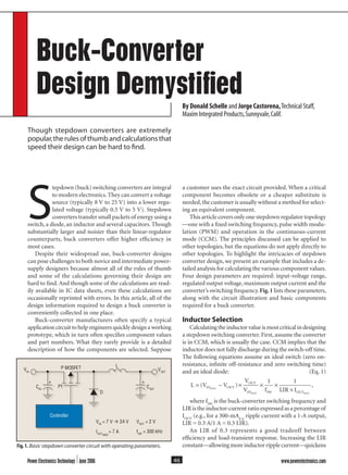
  • 1. Power Electronics Technology June 2006 www.powerelectronics.comJune 2006 www.powerelectronics.com46 Buck-Converter Design Demystified Though stepdown converters are extremely popular,therulesofthumbandcalculationsthat speed their design can be hard to find. By Donald Schelle and Jorge Castorena,Technical Staff,Jorge Castorena,Technical Staff,Jorge Castorena, Maxim Integrated Products,Sunnyvale,Calif. S tepdown (buck) switching converters are integral to modern electronics.They can convert a voltage source (typically 8 V to 25 V) into a lower regu- lated voltage (typically 0.5 V to 5 V). Stepdown converters transfer small packets of energy using a switch, a diode, an inductor and several capacitors. Though substantially larger and noisier than their linear-regulator counterparts, buck converters offer higher efficiency in most cases. Despite their widespread use, buck-converter designs can pose challenges to both novice and intermediate power- supply designers because almost all of the rules of thumb and some of the calculations governing their design are hard to find. And though some of the calculations are read- ily available in IC data sheets, even these calculations are occasionally reprinted with errors. In this article, all of the design information required to design a buck converter is conveniently collected in one place. Buck-converter manufacturers often specify a typical application circuit to help engineers quickly design a working prototype, which in turn often specifies component values and part numbers. What they rarely provide is a detailed description of how the components are selected. Suppose a customer uses the exact circuit provided. When a critical component becomes obsolete or a cheaper substitute is needed,the customer is usually without a method for select- ing an equivalent component. This article covers only one stepdown regulator topology one with a fixed switching frequency, pulse width modu-one with a fixed switching frequency, pulse width modu- lation (PWM) and operation in the continuous-current mode (CCM). The principles discussed can be applied to other topologies, but the equations do not apply directly to other topologies. To highlight the intricacies of stepdown converter design, we present an example that includes a de- tailed analysis for calculating the various component values. Four design parameters are required: input-voltage range, regulated output voltage,maximum output current and the converter’s switching frequency.Fig.1 lists these parameters, along with the circuit illustration and basic components required for a buck converter. Inductor Selection Calculating the inductor value is most critical in designing a stepdown switching converter. First, assume the converter is in CCM, which is usually the case. CCM implies that the inductor does not fully discharge during the switch-off time. The following equations assume an ideal switch (zero on- resistance, infinite off-resistance and zero switching time) and an ideal diode: (Eq. 1) L V V V f LIR I IN OUT OUVOUV T INV fINV fSWV fSWV f OUT MAXMAXMA MAX MSWX MSW OUX MOUTX MTMAX MMA AX L V= −L V × ×× ×OU × ×OUT × ×T × R I×R I ( )L V( )L V V( )VIN( )INL VINL V( )L VINL V OU( )OUVOUV( )VOUV T( )TMA ( )MAX ( )XMAXMA ( )MAXMA = −( )= −L V= −L V( )L V= −L V , 1 1 where fSW where fSW where f is the buck-converter switching frequency and LIR is the inductor-current ratio expressed as a percentage of IOUT (e.g., for a 300-mAp-p (e.g., for a 300-mAp-p (e.g., for a 300-mA ripple current with a 1-A output, LIR = 0.3 A/1 A = 0.3 LIR). An LIR of 0.3 represents a good tradeoff between efficiency and load-transient response. Increasing the LIR constant—allowing more inductor ripple current—quickensFig.1. Basic stepdown converter circuit with operating parameters. Controller P1 VIN VOUT L COUT CIN D P MOSFET VIN = 7 V � 24 V VOUT = 2 V IOUT fSW = 300 kHz MAX = 7 A + +
  • 2. Power Electronics Technology June 2006 www.powerelectronics.comJune 2006 www.powerelectronics.com48 BUCK-CONVERTER DESIGNSBUCK-CONVERTER DESIGNS the load-transient response, and decreasing the LIR con- stant—thereby reducing the inductor ripple current—slows the load-transient response.Fig.2 depicts transient response and inductor current for a given load current, for LIR con- stants ranging from 0.2 to 0.5. Peak current through the inductor determines the inductor’s required saturation-current rating,which in turn dictates the approximate size of the inductor. Saturating the inductor core decreases the converter efficiency, while increasing the temperatures of the inductor, the MOSFET and the diode.You can calculate the inductor’s peak operat- ing current as follows: I I I I LIR I V PEI IPEI IAKI IAKI IOUT INDUCTOR OUI VOUI VT II VT II V MATMAT XMAXMA MAT IMAT IXT IXT IMAXMAT IMAT IXT IMAT I = +I I= +I IOU= +OUT= +T = ×I L= ×I LIR= ×IR I V=I V ∆ ∆ 2 , (I V(I VT I(T II VT II V(I VT II V where INI LINI LDUCTOI LDUCTOI LRI LRI L N ONN ON UT OUT IN SW MAN OMAN OXN OXN OMAXMAN OMAN OXN OMAN O MAXMAXMA VN OVN O VOUVOU V fINV fIN SWV fSW L − ×N O− ×N OUT− ×UT− ×N O− ×N OV− ×VN OVN O− ×N OVN O × ×× × )− ×)− × . 1 1 For the values listed in Fig.1, these equations yield a cal- culated inductance of 2.91 µH (LIR = 0.3).Select an available value that is close to the calculated value, such as a 2.8 µH, and make sure that its saturation-current rating is higher than the calculated peak current (IPEAK = 8.09 A). Choose a saturation-current rating that’s large enough (10Ainthiscase)tocompensateforcircuittolerancesandthe difference between actual and calculated component values. An acceptable margin for this purpose, while limiting the inductor’s physical size, is 20% above the calculated rating. Inductors of this size and current rating typically have a maximum dc resistance range (DCR) of 5 m to 8 m. To minimize power loss, choose an inductor with the lowest possibleDCR.Althoughdatasheetspecificationsvaryamong vendors,always use the maximum DCR specification for de- sign purposes rather than the typical value,because the maxi- mum is a guaranteed worst-case component specification. Output Capacitor Selection Output capacitance is required to minimize the voltage overshoot and ripple present at the output of a stepdown converter.Large overshoots are caused by insufficient output capacitance,and large voltage ripple is caused by insufficient capacitance as well as a high equivalent-series resistance (ESR) in the output capacitor. The maximum allowed output-voltage overshoot and ripple are usually specified at the time of design. Thus, to meet the ripple specification for a stepdown converter circuit, you must include an output capacitor with ample capacitance and low ESR. The problem of overshoot, in which the output-voltage overshoots its regulated value when a full load is suddenly removed from the output, requires that the output capaci- tor be large enough to prevent stored inductor energy from launching the output above the specified maximum output voltage. Output-voltage overshoot can be calculated using the following equation: (Eq. 2)∆ ∆ V VV V L I I C VOUV VOUV V T OU O OUVOUV T MAXMAXMA V V=V V       V VV V                                        −2 2 2 ( )( )∆ ( )∆ L I( )L I I ( )I OU( )OUT( )T IN ( )INDUCTO ( )DUCTOR ( )R MA ( )MATMAT( )TMAT X ( )XMAXMA ( )MAXMA +( )+ 2 ( ) 2 . Rearranging Eq. 2 yields: (Eq. 3)C L I II V O OUT INDUCTOR OUT OVT OV UT MAMATMAT XXMAXMAMAXMA = +  L I  L I  L I  L IL I  L I  L I  L I    L I  L IL I  L I  L I  L IL I  L IL I  L I  L I  L IL I  L I  L I  L I                + −T O+ −T O ∆∆ 22 2 2 + −2 + − 2 ( )V V( )V VOU( )OUV VOUV V( )V VOUV V T O( )T O+ −( )+ −V V+ −V V( )V V+ −V VOU+ −OU( )OU+ −OUV VOUV V+ −V VOUV V( )V VOUV V+ −V VOUV V T O+ −T O( )T O+ −T O∆( )∆ , where CO equals output capacitance and ∆V equals maxi- mum output-voltage overshoot. Setting the maximum output-voltage overshoot to 100 mV and solving Eq. 3 yields a calculated output capaci- tance of 442 µF.Adding the typical capacitor-value tolerance (20%) gives a practical value for output capacitance of ap- proximately 530 µF. The closest standard value is 560 µF. Output ripple due to the capacitance alone is given by: V C V V L V V f OUVOUV T O INV VINV VOUV VOUV V T OUVOUV T INV fINV fSWV fSWV fCATCAT PACITOR MAXMAXMA MAXMAXMA = ×= × V V−V V × ×× ×OU × ×OUT × ×T   × ×× ×                1 2 1 2 . ESR of the output capacitor dominates the output-voltage ripple. The amount can be calculated as follows: V I ESR I ESROUV IOUV IT LV IT LV I C IR IC IR I NDUCTOR CESR CESRR CREST LEST LR RT LR RT L IPPLE OC IE OC I O = ×V I= ×V IT L= ×T LV IT LV I= ×V IT LV I = ×R I= ×R IC I= ×C IR IC IR I= ×R IC IR I N= ×NDUCTO= ×DUCTOR C= ×R CR I= ×R IR IC IR I= ×R IC IR I∆R I∆R IR IC IR I∆R IC IR IR I= ×R I∆R I= ×R IR IC IR I= ×R IC IR I∆R IC IR I= ×R IC IR I . Be aware that choosing a capacitor with very low ESR may cause the power converter to be unstable. The factors that affect stability vary from IC to IC,so when choosing an out- put capacitor, be sure to read the data sheet and pay special attention to sections dealing with converter stability. LIR = 0.2 LIR = 0.3 LIR = 0.4 LIR = 0.5 Fig.2.As LIR increases from 0.2 to 0.5,the load-transient response quickens.The top waveform is the ac-coupled output-voltage ripple,at 100 mV/div.The center waveform is the current load at 5 A/div.And the bottom waveform is the inductor current at 5 A/div.The time scale is 20 µs/div for all waveforms.
  • 3. www.powerelectronics.com Power Electronics Technology June 2006www.powerelectronics.com Power Electronics Technology49 Adding the output-voltage ripple due to capacitance value (the first term in Eq. 4) and the output-capacitor ESR (the second term in Eq. 4) yields the total output-voltage ripple for the stepdown converter: V C V V L V V f I OUVOUV T O INV VINV VOUV VOUV V T OUVOUV T INV fINV fSWV fSWV f INDU RIPPLTRIPPLT E MAXMAXMA MAXMAXMA = ×= × V V−V V × ×× ×OU × ×OUT × ×T   × ×× ×                + 1 2 1 2 ∆ CTORCCTORC CESR O × . (Eq. 4) Rearranging Eq. 4 to solve for ESR yields: ESR I V C V V L V V C INDUCTOR OUVOUV T O INV VINV VOUV VOUV V T OUVOUV T INVINV O RIPPLTRIPPLT E MAXMAXMA MAXMAXMA = ×= × − ×− × V V−V V × 1 1 2 1 ∆ fffSWfffSWfff                                       2 . (Eq. 5) A decent stepdown converter usually achieves an output- voltage ripple of less than 2% (40 mV in our case). For a 560-µF output capacitance, Eq. 5 yields 18.8 mΩ for the maximum calculated ESR. Therefore, choose a capacitor with ESR that’s lower than 18.8 mΩ and a capacitance that’s equal to or greater than 560 µF.To achieve an equivalent ESR value less than 18.8 mΩ, you can connect multiple low-ESR capacitors in parallel. Fig.3 presentsoutput-ripplevoltageversusoutputcapaci- tance and ESR. Because our example uses tantalum capaci- tors, capacitor ESR dominates the output-voltage ripple. Input Capacitor Selection The input capacitor’s ripple-current rating dictates its value and physical size,and the following equation calculates the amount of ripple current the input capacitor must be able to handle: I I V V V C OI IC OI I UT OUV VOUV VT IV VT IV VN OUT INVINVIC OIC ORM C ORM C OS C OS C O MAUTMAUT XMAXMA I I=I I ( )V V( )V V V( )VT I( )T IV VT IV V( )V VT IV VN O( )N OVN OV( )VN OV UT( )UT−( )− . Fig.3.The output capacitor’s equivalent series resistance (ESR) dominates the output-voltage ripple. Fig. 4 plots ripple current for the capacitor (shown as a multiple of the output current) against the input voltage of the buck converter (shown as a ratio of output voltage to input voltage). The worst case occurs when VIN = 2VOUT = 2VOUT = 2V (VOUT (VOUT (V /VIN = 0.5), yielding IOUTMATMAT XMAXMA / 2 for the worst-case ripple-current rating. The input capacitance required for a stepdown converter depends on the impedance of the input power source. For common laboratory power supplies, 10 µF to 22 µF of ca- pacitance per ampere of output current is usually sufficient. Given the design parameters of Fig. 1, you can calculate the input-ripple current as 3.16 A.You then can start with 40 µF in total input capacitance and can adjust that value according to subsequent test results. Tantalum capacitors are a poor choice for input capaci- tors. They usually fail “short,” meaning the failed capaci- tor creates a short circuit across its terminals and thereby raises the possibility of a fire hazard.Ceramic or aluminum- electrolytic capacitors are preferred because they don’t have this failure mode. Ceramic capacitors are the better choice when pc-board area or component height is limited, but ceramics may cause your circuit to produce an audible buzz. This high- pitched noise is caused by physical vibration of the ceramic capacitor against the pc board as a result of the capacitor’s ferroelectric properties and piezo phenomena reacting to the voltage ripple.Polymer capacitors can alleviate this problem. BUCK-CONVERTER DESIGNS ESRCO (�) Output capacitance(F) 0.5 Output-voltageripple(V) 0.4 0.3 0.2 0.1 0 8-10-4 6-10-4 4-10-4 2-10-4 0 0 0.025 0.05 0.075 0.1 More power to you. Helping Engineer the TechnologyTechnologyT of Power www.icecomponents.com • (800) 729-2099 • ISO 9001/9002 Innovative designs. Customs to meet your specific needs. ICE offers an extensive line of gate drive transformers for your high frequency, high density, high isolation or high power requirements. • GT01 - World’s smallest footprint • GT02 - Low profile under 3mm • GT03 - Small SMT package can meet medical safety requirements • GT04 - Thru-hole design for a broad range of applications The Gate Drive TransformerTransformerT For Your Application
  • 4. Power Electronics Technology June 2006 www.powerelectronics.comJune 2006 www.powerelectronics.com50 Polymer capacitors also fail short, but they are much more robust than tantalums, and therefore are suitable as input capacitors. Diode Selection Power dissipation is the limiting factor when choosing a diode. The worst-case average power can be calculated as follows: (Eq. 6) P V V I VDIODPDIODP E OUVOUV T INVINV OUT D MAXMAXMA MAT DMAT DXT DXT DMAXMAT DMAT DXT DMAT D= −   = −= −               1 ,I V1 ,I VOU1 ,OUI VOUI V1 ,I VOUI VT D1 ,T DI VT DI V1 ,I VT DI VT DMAT D1 ,T DMAT D1 ,1 , V 1 , V OU 1 ,OUT 1 ,T T DXT D1 ,T DXT DT DMAT DXT DMAT D1 ,T DMAT DXT DMAT D= −1 ,= −  1 ,   1 ,  1 ,    1 ,       1 ,    × ×1 ,× ×I V× ×I V1 ,I V× ×I VI VOUI V× ×I VOUI V1 ,I VOUI V× ×I VOUI VI VT DI V× ×I VT DI V1 ,I VT DI V× ×I VT DI V where VD is the voltage drop across the diode at the given output current IOUTMATMAT XMAXMA . (Typical values are 0.7 V for a silicon diode and 0.3V for a Schottky diode.) Ensure that the selected diode will be able to dissipate that much power. For reliable operation over the input-voltage range, you must also ensure that the reverse-repetitive maximum voltage is greater than the maximum input voltage (VRRM  VINVINV MAXMAXMA ). The diode’s forward-current specification must meet or exceed the maximum output current (i.e.,IFAVFAVF  IOUTMATMAT XMAXMA ). MOSFET Selection Selecting a MOSFET can be daunting, so engineers often avoid that task by choosing a regulator IC with an internal MOSFET. Unfortu- nately, most manufacturers find it cost prohibitive to integrate a large MOSFET withadc-dccontrollerinthesamepack- age,so power converters with integrated MOSFETs typically specify maximum output currents no greater than 3 A to 6 A. For larger output currents, the only alternative is usually an external MOSFET. The maximum junction tempera- ture ( TJTJTMAXMAXMA ) and maximum ambient temperature ( TATAT MAXMAXMA ) for the external MOSFETmustbeknownbeforeyoucan select a suitable device. TJTJTMAXMAXMA should not exceed 115o C to 120o C and TATAT MAXMAXMA should not exceed 60o C. A 60o C maximum ambient temperature may seem high, but stepdown converter circuits are typically housed in a chassis where such ambient temperatures are not unusual. You can calculate a maximum allow- able temperature rise for the MOSFET as follows: T T TJ JT TJ JT T ATATRISEJ JRISEJ JMAX MAX MAMAX MMA AX = −T T= −T T . (Eq. 7) Insertingthevaluesmentionedabove for TJTJTMAXMAXMA and TATAT MAXMAXMA into Eq. 7 yields a maximum MOSFET temperature rise of 55o C. The maximum power dissi- pated in the MOSFET can be calculated from the allowable maximum rise in MOSFET temperature: (Eq. 8)(Eq. 8)P (Eq. 8)P (Eq. 8) T (Eq. 8)D (Eq. 8)(Eq. 8)P (Eq. 8)D (Eq. 8)P (Eq. 8) J (Eq. 8) J (Eq. 8) TJT JA TO (Eq. 8)TO (Eq. 8)T (Eq. 8)T (Eq. 8) RISE (Eq. 8) RISE (Eq. 8)(Eq. 8)= (Eq. 8) Θ (Eq. 8) Θ (Eq. 8)(Eq. 8). (Eq. 8) The type of MOSFET package and the amount of pc-board copper con- nected to it affect the MOSFET’s junc- tion-to-ambient thermal resistance (JA ). When JA is not specified in the data sheet,62o C/W serves as a good esti- mate for a standard SO-8 package (wire- bond interconnect, without an exposed BUCK-CONVERTER DESIGNSBUCK-CONVERTER DESIGNS TM 10 to 125 kHz Hard Switching Insulated Gate Bipolar Transistors ADVANCED POWER TECHNOLOGY IS NOW Phone: (541)382-8028 www.microsemi.com Power MOS 7® IGBTs (600, 900, 1200V) PT Technology Ultralow Gate Resistance and Charge Ultralow Switching Losses Low Cost Alternative to MOSFETs Excellent Noise Immunity Combi with High Speed Diode Available Field Stop IGBTs (600 & 1200V) Trench Technology Short Circuit Rated Very Low Conduction Losses Easy Paralleling Combi with High Speed Diode Available Thunderbolt® IGBTs (600 & 1200V) NPT Technology Short Circuit Rated Moderate to High Frequency Easy Paralleling Combi with High Speed Diode Available
  • 5. Power Electronics Technology June 2006 www.powerelectronics.comJune 2006 www.powerelectronics.com52 BUCK-CONVERTER DESIGNSBUCK-CONVERTER DESIGNS paddle), mounted on 1 in.2 of 1-oz pc-board copper. There exists no inverse linear relationship between a jA value and the amount of copper connected to the device,and the benefit of decreasing the JAJAJ value quickly dwindles for circuits that include more than 1 sq in. of pc-board copper. Using JA = 62JA = 62JA ° C/W in Eq.8 yields a maximum allowable dis- sipated power in the MOSFET of approximately 0.89 W. Power dissipation in the MOSFET is caused by on- resistance and switching losses. On-resistance loss can be calculated as: (Eq. 9)P (Eq. 9)P (Eq. 9)V (Eq. 9)V (Eq. 9) V I R (Eq. 9)I R (Eq. 9) DPDP (Eq. 9)OU (Eq. 9)(Eq. 9)V (Eq. 9)OU (Eq. 9)V (Eq. 9)(Eq. 9)T (Eq. 9) INVINV OUI ROUI RT DI RT DI R S O HOTRDS MIN MAT DMAT DXT DXT DMAXMAT DMAT DXT DMAT D= × (Eq. 9)= × (Eq. 9)(Eq. 9)= × (Eq. 9)(Eq. 9)OU (Eq. 9)= × (Eq. 9)OU (Eq. 9)(Eq. 9)T (Eq. 9)= × (Eq. 9)T (Eq. 9)I R×I R (Eq. 9)I R (Eq. 9)× (Eq. 9)I R (Eq. 9)I RT DI R×I RT DI R (Eq. 9)2 (Eq. 9)(Eq. 9)I R (Eq. 9)2 (Eq. 9)I R (Eq. 9) ( )S O( )S ON( )N . Because most data sheets specify the maximum on- resistance only at 25°C, you may have to estimate the value of on-resistance at TJTJTHOT . As a rule of thumb, a temperature coefficient of 0.5%/°C provides a good indicator for maxi- mum on-resistance at any given temperature. Thus, the hot on-resistance is calculated as: (Eq. 10) R T C RDSR TDSR THOT J DC RJ DC R S O CHOJ DHOJ DTJ DTJ D( )R T( )R TON( )ONR TONR T( )R TONR T ( )S O( )S ON( )N[ .R T[ .R T( )R T( )R T C R( )C RJ D( )J DR TJ DR T( )R TJ DR T C RJ DC R( )C RJ DC RJ DHOJ D( )J DHOJ DJ DTJ D( )J DTJ D] .C R] .C RJ D] .J DC RJ DC R] .C RJ DC R S O] .S O C ] .C( )] .( )S O( )S O] .S O( )S ON( )N] .N( )NR T= +R TR T[ .R T= +R T[ .R T( )− °( ) ° ] .° ] .[ .1 0[ .R T[ .R T1 0R T[ .R TR T[ .R T= +R T[ .R T1 0R T[ .R T= +R T[ .R T005R T005R T( )25( )J D( )J D25J D( )J D( )− °( )25( )− °( ) 25 ] .25 ] . Assuming the on-resistance loss is approximately 60% of the total MOSFET losses, you can substitute in Eq. 10 and rearrange to yield Eq. 11, the maximum allowable on- resistance at 25°C: (Eq. 11) R V V I T P DS C INVINV OU (Eq. 11) OU (Eq. 11) VOUV T (Eq. 11) T (Eq. 11) OUI TOUI TT JI TT JI TT JI TT JI T DPDP MIN MAT JMAT JX HT JX HT JMAX HMAT JMAT JX HT JMAT J OT TO ( )ON( )ON [ .I T[ .I TT J[ .T JI TT JI T[ .I TT JI TT JX HT J[ .T JX HT J( )I T( )I T C( )CT J( )T JI TT JI T( )I TT JI TX H ( )X HT JX HT J( )T JX HT J OT ( )OT ] 25 2 I T2 I T 1 (Eq. 11) 1 (Eq. 11) I T[ .I T1 0I T[ .I TT J[ .T J1 0T J[ .T JI TT JI T[ .I TT JI T1 0I TT JI T[ .I TT JI TI T005I TT J005T J( )25( ) ° = ×= ×MI = ×MIN = ×N I T+ ×I TI TT JI T+ ×I TT JI TI T+ ×I TI TT JI T+ ×I TT JI TI T[ .I T+ ×I T[ .I TI TT JI T[ .I TT JI T+ ×I TT JI T[ .I TT JI TI T[ .I T1 0I T[ .I T+ ×I T[ .I T1 0I T[ .I TI TT JI T[ .I TT JI T1 0I TT JI T[ .I TT JI T+ ×I TT JI T[ .I TT JI T1 0I TT JI T[ .I TT JI TI T005I T+ ×I T005I TI TT JI T005I TT JI T+ ×I TT JI T005I TT JI T( )− °( )( )25( )− °( )25( ) TTT × 60%. Switching losses constitute a smaller portion of the MOSFET’s power dissipation, but they still must be taken into account. The following switching-loss calculation provides only a rough estimate, and therefore is no substi- tute for evaluation in the lab, preferably a test that includes a thermocouple mounted on P1 as a sanity check. (Eq. 12)(Eq. 12)P (Eq. 12)P (Eq. 12) C V f I I (Eq. 12) I (Eq. 12)(Eq. 12)D (Eq. 12)(Eq. 12)P (Eq. 12)D (Eq. 12)P (Eq. 12) RS (Eq. 12) RS (Eq. 12) C VRSC VS I (Eq. 12) S I (Eq. 12) C VS IC VN S (Eq. 12) N S (Eq. 12) f IN Sf IW Of IW Of I UT GATE SW (Eq. 12)SW (Eq. 12)(Eq. 12) MA (Eq. 12) N SMAN S (Eq. 12) N S (Eq. 12) MA (Eq. 12) N S (Eq. 12) X M (Eq. 12) X M (Eq. 12) N SX MN S (Eq. 12) N S (Eq. 12) X M (Eq. 12) N S (Eq. 12) W OX MW O (Eq. 12) W O (Eq. 12) X M (Eq. 12) W O (Eq. 12) UTX MUT (Eq. 12) UT (Eq. 12) X M (Eq. 12) UT (Eq. 12)(Eq. 12) MA (Eq. 12) X M (Eq. 12) MA (Eq. 12) N SMAN SX MN SMAN S (Eq. 12) N S (Eq. 12) MA (Eq. 12) N S (Eq. 12) X M (Eq. 12) N S (Eq. 12) MA (Eq. 12) N S (Eq. 12) AX (Eq. 12) AX (Eq. 12)(Eq. 12)= (Eq. 12) × ×C V× ×C VS I× ×S IC VS IC V× ×C VS IC VN S× ×N Sf I×f If IW Of I×f IW Of I2 × ×2 × × (Eq. 12), (Eq. 12) where CRSS is the reverse-transfer capacitance of P1, IGATE is the peak gate-drive source/sink current of the controller and P1 is the high-side MOSFET. Assuming a gate drive of 1 A (obtained from the gate driver/ controller data sheet) and a reverse-transfer capaci- tance of 300 pF (obtained from the MOSFET data sheet), Eq. 11 yields a maximum RDS C( )ON( )ON 25° of approximately 26.2 m. Recalculating and summing the on-resistance losses and the switching losses yields a net dissipated power of 0.676 W. Using this figure, you can calculate for the MOSFET a maximum temperature rise of 101o C, which is within the acceptable temperature range. Stepdown-Converter Efficiency Minimizing power loss throughout the converter will extend battery life and reduce heat dissipation. The follow- ing equations calculate power loss in each section of the converter. Input capacitor ESR loss: P I ESRC CP IC CP I CIC CIC CRM C CRM C CS C CS C CIRMS I = ×P I= ×P IC C= ×C CP IC CP I= ×P IC CP I 2 = ×2 = × . Refer to Eqs. 6, 9 and 12 for losses due to the diode, the RM Refer to Eqs. 6, 9 and 12 for losses due to the diode, the RMS Refer to Eqs. 6, 9 and 12 for losses due to the diode, the S RM Refer to Eqs. 6, 9 and 12 for losses due to the diode, the RMS Refer to Eqs. 6, 9 and 12 for losses due to the diode, the S MOSFET on-resistance and the MOSFET switching loss. Inductor DCR loss: P I I DCRDCP IDCP IR OP IR OP I INDUCTOR LI DR LI DCRR LCRRMR ORMR OS MR OS MR OUTS MUT AX P I= +P IP IR OP I= +P IR OP I I D× ×I DI DR LI D× ×I DR LI D( )( )P I( )P I I D( )I DI D( )I DR O( )R OUT( )UT IN( )INI DINI D( )I DINI DDUCTO( )DUCTOI DDUCTOI D( )I DDUCTOI DR L( )R LR L( )R LI DR LI D( )I DR LI DI DR LI D( )I DR LI DS M ( )S MR OS MR O( )R OS MR OUTS MUT( )UTS MUT AX ( )AX = +( )= +P I= +P I( )P I= +P IR O= +R O( )R O= +R OP IR OP I= +P IR OP I( )P IR OP I= +P IR OP I UT= +UT( )UT= +UT I D× ×I D( )I D× ×I DI DR LI D× ×I DR LI D( )I DR LI D× ×I DR LI DI D× ×I D( )I D× ×I DI D× ×I D( )I D× ×I DI DR LI D× ×I DR LI D( )I DR LI D× ×I DR LI DI DR LI D× ×I DR LI D( )I DR LI D× ×I DR LI D .( )∆( )I D( )I D2I D( )I DI DR LI D( )I DR LI D2I DR LI D( )I DR LI DI D× ×I D( )I D× ×I D2I D× ×I D( )I D× ×I DI DR LI D× ×I DR LI D( )I DR LI D× ×I DR LI D2I DR LI D× ×I DR LI D( )I DR LI D× ×I DR LI D2 I D2 I DI D× ×I D2 I D× ×I D Output capacitor ESR loss:Output capacitor ESR loss: P I ESRC IP IC IP I NDUCTOR CESR CESRR CROC IOC IRM C IRM C IS C IS C I O P I= ×P IP IC IP I= ×P IC IP I ×R C×R C( )( )P I( )P IC I( )C IP IC IP I( )P IC IP I N( )NDUCTO( )DUCTOR C( )R CR C( )R C= ×( )= ×P I= ×P I( )P I= ×P IC I= ×C I( )C I= ×C IP IC IP I= ×P IC IP I( )P IC IP I= ×P IC IP I N= ×N( )N= ×NDUCTO= ×DUCTO( )DUCTO= ×DUCTOR C= ×R C( )R C= ×R C .( )∆( )P I( )P I∆P I( )P IP IC IP I( )P IC IP I∆P IC IP I( )P IC IP IP I= ×P I( )P I= ×P I∆P I= ×P I( )P I= ×P IP IC IP I= ×P IC IP I( )P IC IP I= ×P IC IP I∆P IC IP I= ×P IC IP I( )P IC IP I= ×P IC IP I( )3( )R C( )R C3R C( )R C 2 Pc-board copper Loss: Pc-board copper loss is difficult to calculate accurately, but Fig. 5 provides a rough estimate of the amount of resistance per square area of pc-board cop- per. With Fig. 5, you can use a simple I2 R power dissipation equation to calculate the power loss. The following equation sums all of the power losses throughout the converter, and accounts for those losses in the expression for converter efficiency: =(VOUT =(VOUT =(V  IOUT )/(VOUT )/(VOUT )/(V  IOUT + P P PC CP PC CP P DCPDCP RIC CIC CRM C CRM C CS C CS C CORMS RMS + +P P+ +P PC C+ +C CP PC CP P+ +P PC CP P + P P P PD DP PD DP P DIODP PDIODP PE CP PE CP P URDD DRDD DS SD DS SD D W + +P P+ +P PD D+ +D DP PD DP P+ +P PD DP P + ×P P+ ×P PE C+ ×E CP PE CP P+ ×P PE CP P U+ ×U ) %+ ×) %+ × .) %100) % Assuming a reasonable net copper loss of approximately h l b R = ρ x b x h l b = l R = ρ = 1.72 x 10⁻⁸ x mΩ h 1.4 mil R = 0.484 mΩ =~ 0.5 mΩ Fig.5.The resistance of one square of 1-oz copper is approximately 0.5 m. Fig.4.Ripple current for the input capacitors reaches a worst case of IOUT /2 = 0.5 when the variable input voltage equals twice the fixed output voltage. 0 0.1 0.2 0.3 0.4 0.5 0 0.25 0.5 0.75 1 VOUT /VIN Ripplecurrent(multipleofIOUT )
  • 6. www.powerelectronics.com Power Electronics Technology June 2006www.powerelectronics.com Power Electronics Technology53 0.75 W, the efficiency for this converter is 69.5%. Replacing the silicon diode with a Schottky diode increases the ef- ficiency to 79.6%, and replacing the diode with a MOSFET synchronous rectifier further increases the efficiency to 85% at full load. Fig. 6 depicts a breakdown of power losses in the con- verter. Doubling the copper weight to 2 oz or tripling it to 3 oz minimizes the copper loss and thereby increases the efficiency to approximately 86% to 87%. Careful pc-board layout is critical in achieving low switch- ing losses and stable operation for a stepdown converter.Use the following guidelines as a starting point: ● Keep the high-current paths short, especially at the ground terminals. ● Minimize connection lengths to the inductor,MOSFET and diode/synchronous MOSFET. ● Keep power traces and load connections short and wide. This practice is essential for high efficiency. ● Keep voltage- and current-sensing nodes and traces away from switching nodes. Verifying Performance When designing or modifying a stepdown switching- regulator circuit (one that operates in CCM, using PWM), you can use the equations in this article to calculate values for the critical components and characteristics required.You should always lab-test the circuit to verify final electrical and thermal specifications. For acceptable circuit operation, a properpc-boardlayoutandjudiciouscomponentplacements are as critical as choosing the right components. PETech Diode 63% MOSFET switching 5% MOSFET on- resistance 6% Inductor dc resistance 8% 0utput capacitor ESR 7% Copper 8% Input capacitor ESR 3% Fig.6.Power loss caused by the freewheeling diode should be eliminated to increase the converter’s efficiency. BUCK-CONVERTER DESIGNS